Manufacturing method for leadframe and for semiconductor package using the leadframe

a manufacturing method and leadframe technology, applied in the manufacture of cables/conductor devices, solid-state devices, semiconductor devices, etc., can solve the problems of excessive narrowing of lead pitch, physical limitations of lead pitch narrowing during the manufacture of leadframes, and susceptibility to solder shorting between, so as to facilitate the formation of leads and die paddles of leadframes. , the effect of leadframe lead formation

Active Publication Date: 2006-12-05
AMKOR TECH SINGAPORE HLDG PTE LTD
View PDF262 Cites 9 Cited by
  • Summary
  • Abstract
  • Description
  • Claims
  • Application Information

AI Technical Summary

Benefits of technology

[0010]In accordance with the present invention, there is provided a method for fabricating a leadframe having a die paddle and two or more sets of leads which extend at least partially about the die paddle in spaced relation thereto and to each other. In one embodiment of the present invention, the formation of the leads of the leadframe is facilitated by the completion of a chemical etching process to the leadframe subsequent to the application and patterning of a photo resist applied thereto. In another embodiment of the present invention, the formation of both the leads and the die paddle of the leadframe is facilitated through the completion of a chemical etching process subsequent to the application and patterning of a photo resist applied to the leadframe. The electrical isolation of the leads of the leadframe from each other from the die paddle through the implementation of an etching process eliminates the need for the completion of a sawing process as is often used in the fabrication of prior art semiconductor packages including leads arranged in multiple rows and columns.

Problems solved by technology

Although it has been suggested in the prior art to narrow the pitch of the leads formed at the periphery of the bottom surface of the package body to increase the number of leads, there are physical limitations in narrowing the lead pitch during the manufacture of the leadframe.
Also, excessive narrowing in the lead pitch gives rise to a susceptibility of solder shorting between the leads when the semiconductor package is connected to an external device through the use of solder.
In these semiconductor packages, the sawing process gives rise to frequent occurrences of chip-out in the package body, as well as the formation of minute cracks in the leads.
As a result, the completed semiconductor package may have a weakened mechanical structure.
Moreover, the partial cutting of the package body as occurs during the sawing of the leadframe to facilitate the formation of the leads is somewhat unsightly due to the resultant grooves or scratches formed in the corresponding surface of the package body.
Further difficulties arise as a result of the mechanical stresses applied to the package body during the sawing process.

Method used


Image

  • Manufacturing method for leadframe and for semiconductor package using the leadframe
  • Manufacturing method for leadframe and for semiconductor package using the leadframe
  • Manufacturing method for leadframe and for semiconductor package using the leadframe

Examples


first embodiment

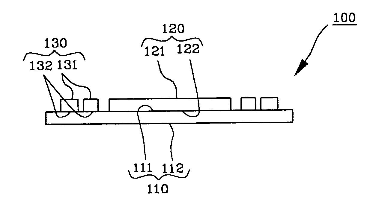
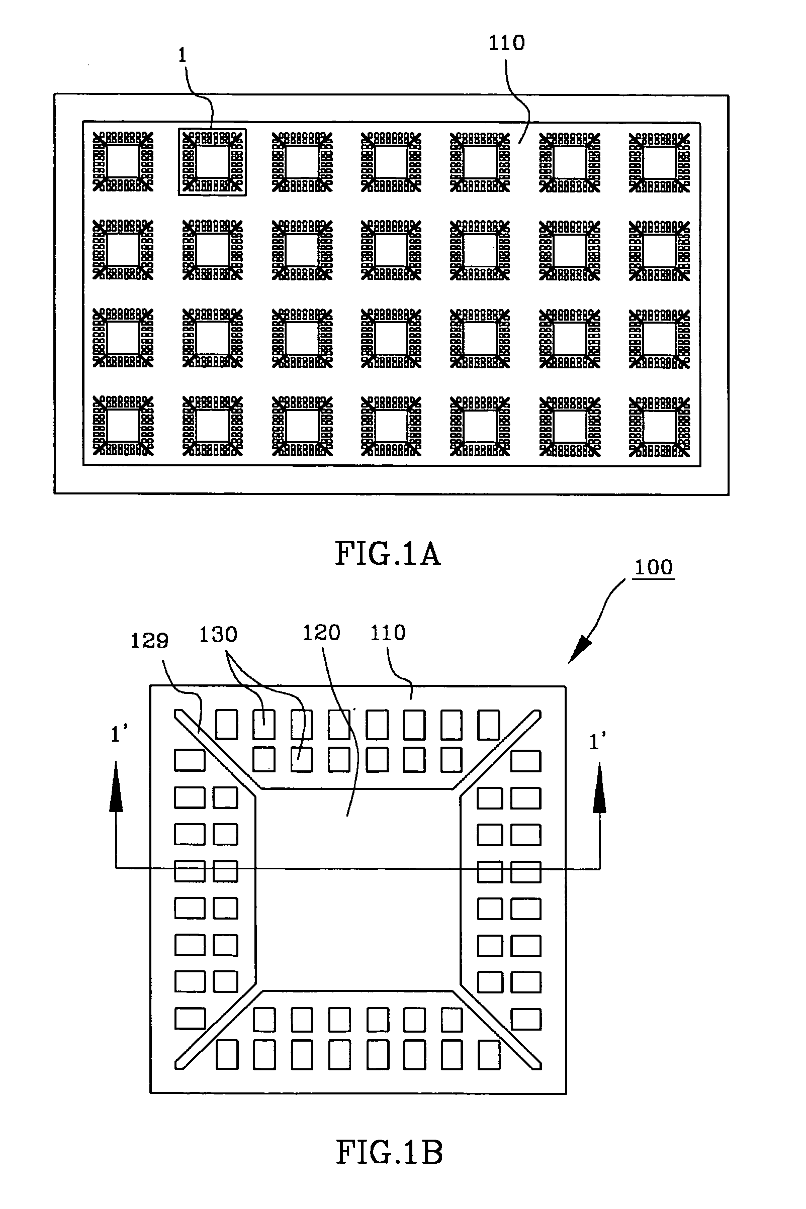
[0025]Referring now to the drawings wherein the showings are for purposes of illustrating preferred embodiments of the present invention only, and not for purposes of limiting the same, FIG. 1A is a top plan view of a leadframe strip having multiple leadframes 100 which are each formed in accordance with the present invention disposed thereon. The leadframe strip comprises a layer of adhesive tape 110. The adhesive tape 110 has a generally planar first (top) surface 111 which has an adhesive property. In addition to the first surface 111, the adhesive tape 110 defines a generally planar second (bottom) surface 112 which is opposite the first surface 111. The adhesive tape may be fabricated from cellophane, vinyl, polyimide, or an equivalent, the present invention not being limited to any particular material for the adhesive tape 110.

[0026]As seen in FIG. 1A, multiple leadframes 100 are adhesively secured to the first surface 111 of the adhesive tape 110 in a matrix-like pattern defi...

second embodiment

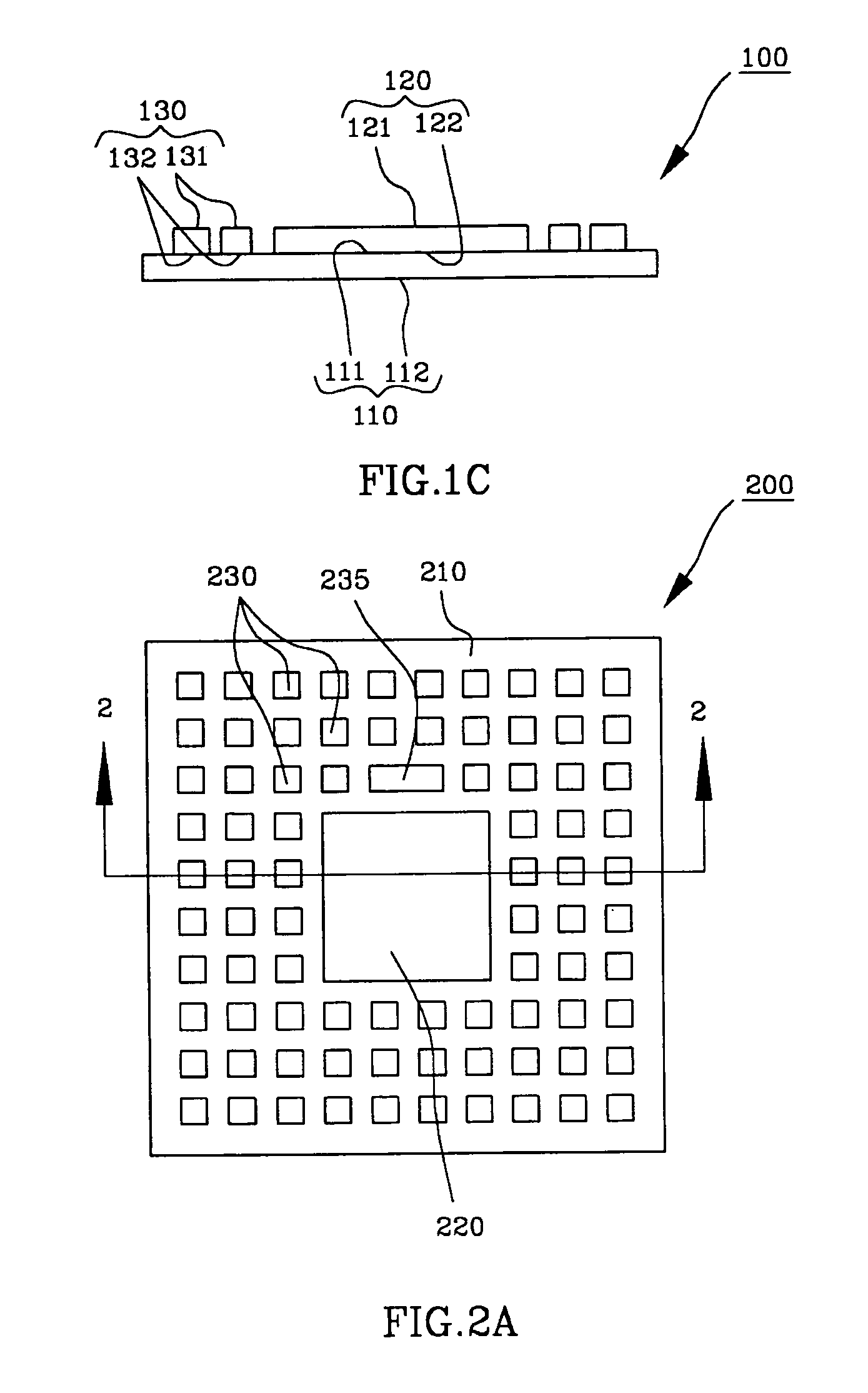
[0039]Referring now to FIGS. 2A and 2B, there is shown a leadframe 200 which is formed in accordance with the present invention. In FIGS. 2A and 2B, the 200 series reference numerals are used to identify elements corresponding to those identified with the 100 series reference numerals shown in FIGS. 1A–1C. One of the distinctions between the leadfarmes 100, 200 lies in the omission in the leadframe 200 of the tie bars 129 described above in relation to the leadframe 100. A further distinction lies in the number and arrangement of leads 230 in the leadframe 200 in comparison to the number and arrangement of leads 130 in the leadframe 100. More particularly, in the leadframe 200, the leads 230 are arranged in an inner set which circumvents the die paddle 220, a middle set which circumvents the inner set, and an outer set which circumvents the middle set. Due to the absence of the above-described tie bars 129 in the leadframe 200, leads 230 of the inner, middle and outer sets are arran...


PUM

PropertyMeasurementUnit
areaaaaaaaaaaa
electricallyaaaaaaaaaa
conductiveaaaaaaaaaa

Abstract

In accordance with the present invention, there is provided a method for manufacturing a leadframe. The method comprises the initial step of bonding a primary leadframe to an adhesive tape layer, the primary leadframe including a die paddle and a plurality of leads which extend at least partially about the die paddle in spaced relation thereto. Thereafter, a photo resist is applied to the primary leadframe and to the adhesive tape layer. The photo resist is then patterned to define at least one exposed area in each of the leads of the primary leadframe. The exposed areas of the leads are then etched to divide the leads into an inner set which extends at least partially about the die paddle and an outer set which extends at least partially about the inner set. Thereafter, the photo resist is removed from the die paddle and from the inner and outer sets of the leads.

Description

CROSS-REFERENCE TO RELATED APPLICATIONS[0001]Not ApplicableSTATEMENT RE: FEDERALLY SPONSORED RESEARCH / DEVELOPMENT[0002]Not ApplicableBACKGROUND OF THE INVENTION[0003]1. Field of the Invention[0004]The present invention relates generally to semiconductor packages, and more particularly to a method of manufacturing a semiconductor package which includes a plurality of leads arranged in multiple columns and rows.[0005]2. Description of the Related Art[0006]Semiconductor dies are conventionally enclosed in plastic packages that provide protection from hostile environments and enable electrical interconnection between the semiconductor die and an underlying substrate such as a printed circuit board (PCB) or motherboard. The elements of such a package include a metal leadframe, an integrated circuit or semiconductor die, bonding material to attach the semiconductor die to the leadframe, bond wires which electrically connect pads on the semiconductor die to individual leads of the leadfram...

Claims


Application Information

Patent Timeline
Patent Type & Authority Patents(United States)
IPC IPC(8): H01B13/00B44C1/22
CPCH01L21/568H01L21/6835H01L2224/48091H01L2224/48247H01L2924/01046H01L2924/01078H01L2924/01079H01L2924/00014H01L2224/45124H01L2224/45144H01L2224/45147H01L24/45H01L2224/73265H01L2224/92247H01L2224/32245H01L2924/14H01L2924/181H01L2924/00H01L2924/00012
Inventor YANG, SUNG JINMOON, DOO HWAN
Owner AMKOR TECH SINGAPORE HLDG PTE LTD
Why Eureka
Try Eureka