Methods to improve the SiGe heterojunction bipolar device performance

a bipolar transistor and heterojunction technology, applied in the field of bipolar transistors, can solve the problems of serious device operational limitations, and achieve the effect of improving bipolar performance and improving bipolar performan

a bipolar transistor and heterojunction technology, applied in the field of bipolar transistors, can solve the problems of serious device operational limitations, and achieve the effect of improving bipolar performance and improving bipolar performan

US7144787B2Active Publication Date: 2006-12-05IBM CORP

Image

  • Methods to improve the SiGe heterojunction bipolar device performance
  • Methods to improve the SiGe heterojunction bipolar device performance
  • Methods to improve the SiGe heterojunction bipolar device performance

Examples


Embodiment Construction

[0034]The present invention, which provides methods to improve the bipolar device performance as well as the resultant structure produced by the inventive methods, will now be described in more detail by referring to the drawings that accompany the present application. The drawings are provided for illustrative purposes and are thus not drawn to scale.

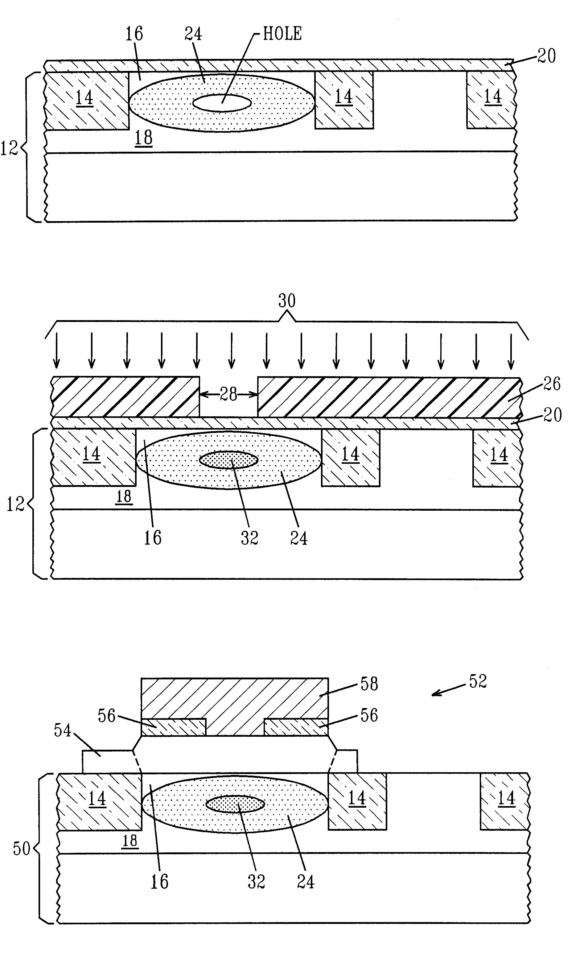
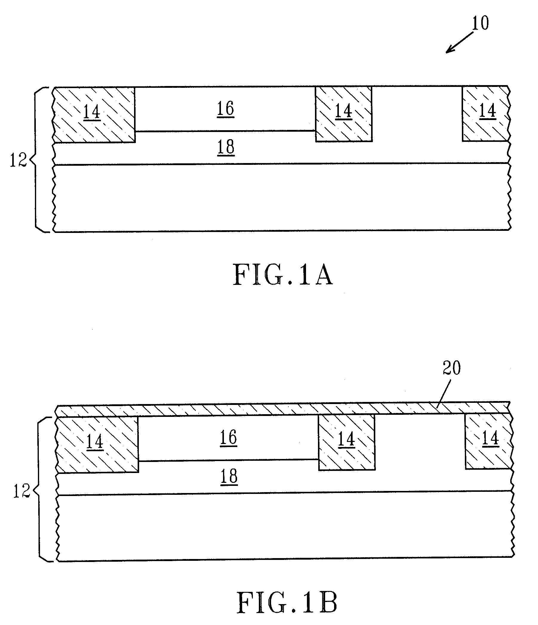
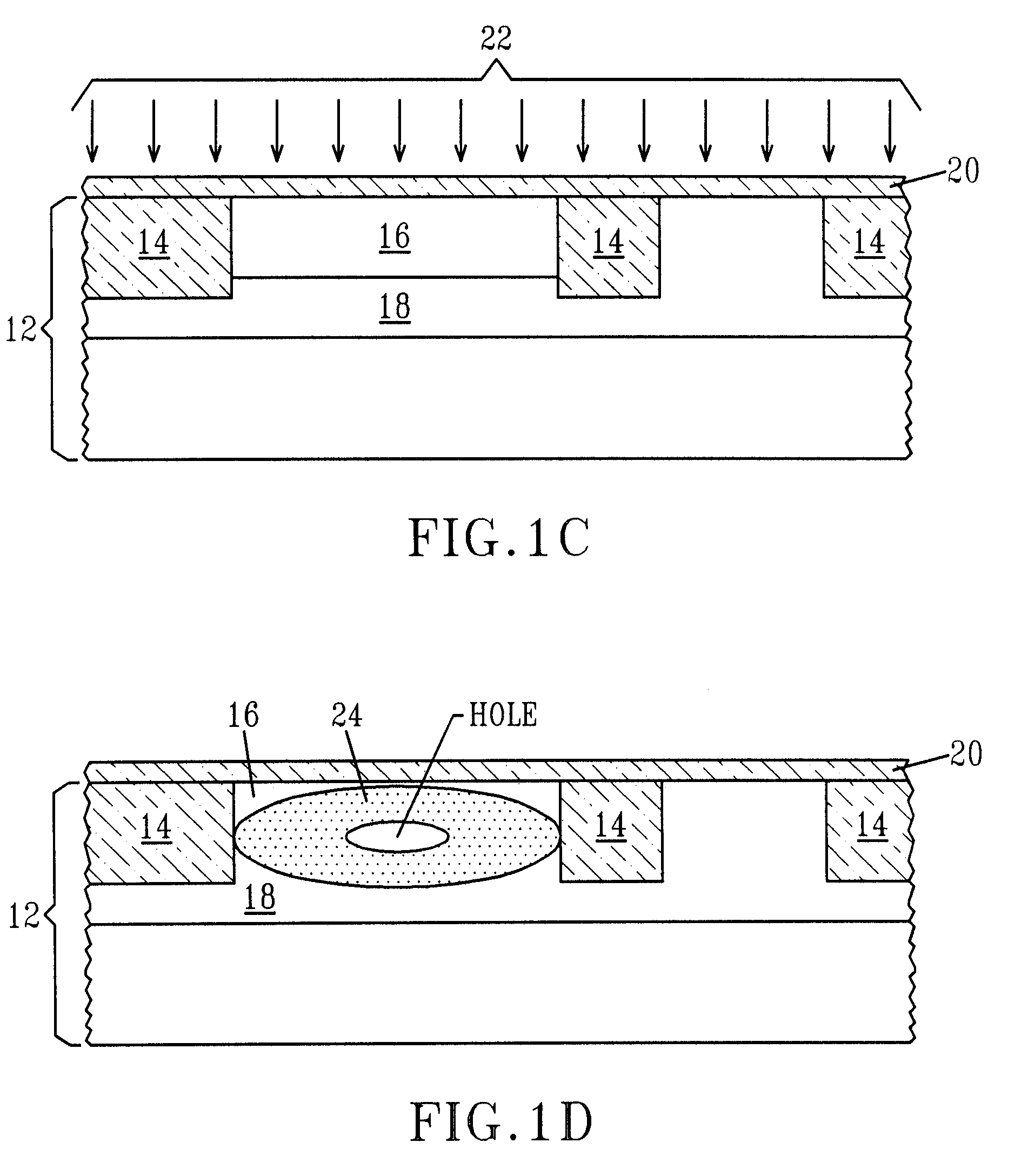
[0035]FIGS. 1A–1F are pictorial representations illustrating the basic processing steps that are employed in one embodiment of the present invention for forming a semiconductor structure which can be used to boost the performance of a bipolar transistor. FIG. 1A shows an initial structure 10 that can be used in the present invention. The initial structure 10 includes a Si-containing substrate 12 having trench isolation regions 14 formed therein. The Si-containing substrate 12 comprises any semiconductor material that includes silicon. Illustrative examples of such Si-containing materials that can be used as substrate 12 include, but ar...


PUM


Abstract

Methods of boosting the performance of bipolar transistor, especially SiGe heterojunction bipolar transistors, is provided together with the structure that is formed by the inventive methods. The methods include providing a species-rich dopant region comprising C, a noble gas, or mixtures thereof into at least a collector. The species-rich dopant region forms a perimeter or donut-shaped dopant region around a center portion of the collector. A first conductivity type dopant is then implanted into the center portion of the collector to form a first conductivity type dopant region that is laterally constrained, i.e., confined, by the outer species-rich dopant region.

Description

FIELD OF THE INVENTION[0001]The present invention generally relates to bipolar transistors and, more particularly, to methods of fabricating a substrate for a heterojunction bipolar transistor (HBT) in which ion implantation is employed to improve the performance of the bipolar device. The present invention also relates to a substrate that can be used for providing a bipolar device that exhibits improved device performance.BACKGROUND OF THE INVENTION[0002]Bipolar transistors are devices with two p-n junctions that are in close proximity to each other. A typical bipolar transistor has three device regions: an emitter, a collector, and a base disposed between the emitter and the collector. Ideally, the two p-n junctions, i.e., the emitter-base and collector-base junctions, are in a single layer of semiconductor material separated by a specific distance. Modulation of the current flow in one p-n junction by changing the bias of the nearby junction is called “bipolar-transistor action.”...

Claims


Application Information

Patent Timeline
05 Dec 2006
Publication
US7144787B2
IPC
H01L21/331
CPC
H01L29/0821; H01L29/66242; H01L29/7378
Inventors
DOKUMACI, OMER H.; FREEMAN, GREGORY G.