
Method of semiconductor nanoparticle synthesis

a technology of nanoparticles and nanoparticles, applied in the field of nanoparticles, can solve the problems of unacceptably low quantum yield of most applications, high degree of polydispersity, and high degree of internal defects, so as to stop the growth of nanoparticles, and stop the growth of shells

Inactive Publication Date: 2006-12-12
INVITROGEN
View PDF12 Cites 76 Cited by
  • Summary
  • Abstract
  • Description
  • Claims
  • Application Information

AI Technical Summary

Benefits of technology

[0009]One aspect of the invention relates to a method of producing nanoparticles comprising: (a) mixing a first precursor and at least one coordinating solvent to form a first mixture; (b) exposing the first mixture to a reaction promoter selected from the group consisting of oxygen and a reducing agent; (c) heating the first mixture to a temperature that is sufficiently high to form nanoparticles (nucleation crystals) when a second precursor is added; (d) introducing a second precursor into the first mixture to form a second mixture thereby resulting in the formation of a plurality of nanoparticles; and (e) cooling the second mixture to stop further growth of the nanoparticles.
[0010]Another embodiment of the invention is a method of producing nanoparticles comprising: (a) mixing a first precursor and a second precursor with at least one coordinating solvent to form a first mixture; (b) heating the first mixture to a temperature that is sufficiently high to form nanoparticles when a reaction promoter is added; (c) exposing the first mixture to a reaction promoter, the reaction promoter being selected from the group consisting of oxygen and a reducing agent, to form a second mixture thereby resulting in the formation of a plurality of nanoparticles; and (d) cooling the second mixture to stop further growth of the nanoparticles.
[0011]Yet another embodiment of the invention is a method of producing the nanoparticle shell comprising (a) mixing nanoparticles with at least one coordinating solvent to form a first mixture; (b) heating the first mixture to a temperature that is sufficiently high to form a shell on the nanoparticles when first and second precursors are added; (c) introducing first and second precursors into the first mixture to form a second mixture thereby resulting in the formation of shells on a plurality of nanoparticles; and (d) cooling the second mixture to stop further growth of the shell; wherein the method further comprises exposing the first or second mixture to a reaction promoter selected from the group consisting of oxygen and a reducing agent. The nanoparticles can be produced by the methods described herein or can be produced by any method known in the art.
[0012]Another aspect of the invention pertains to a method of producing semiconductive nanoparticles having a valency “n”, comprising: (a) mixing a first precursor having a valency “c” and at least one coordinating solvent to form a mixture; (b) exposing the mixture to a reaction promoter wherein the reaction promoter converts the valency of the first precursor to a valency “a”; (c) heating the mixture to a temperature that is sufficiently high to form nanoparticles when a second precursor is added; (d) introducing a second precursors into the mixture to form a second mixture thereby resulting in the formation of a plurality of nanoparticles; wherein the second precursor has a valency “b”, and wherein a+b=n and c+b≠n; and (e) cooling the second mixture to stop further growth of the nanoparticles.

Problems solved by technology

The two former methods yield particles that have unacceptably low quantum yields for most applications, a high degree of polydispersity, poor colloidal stability, a high degree of internal defects, and poorly passivated surface trap sites.
In addition, nanocrystals made by the first route are physically confined to a glass matrix and cannot be further processed after synthesis.
Unfortunately, it is difficult to optimize the particle yield, while maintaining the desirable features of the Cd(II) synthesis conditions.
In particular, for smaller size nanoparticle synthesis, yields have been very poor under Cd(II) synthesis conditions.
Reaction conditions that provide such low yields are not only more expensive to implement on a manufacturing scale, but they often require much larger reactors and produce more hazardous waste.

Method used


Image

  • Method of semiconductor nanoparticle synthesis
  • Method of semiconductor nanoparticle synthesis
  • Method of semiconductor nanoparticle synthesis

Examples


example 1

Reactions with Phosphines Added

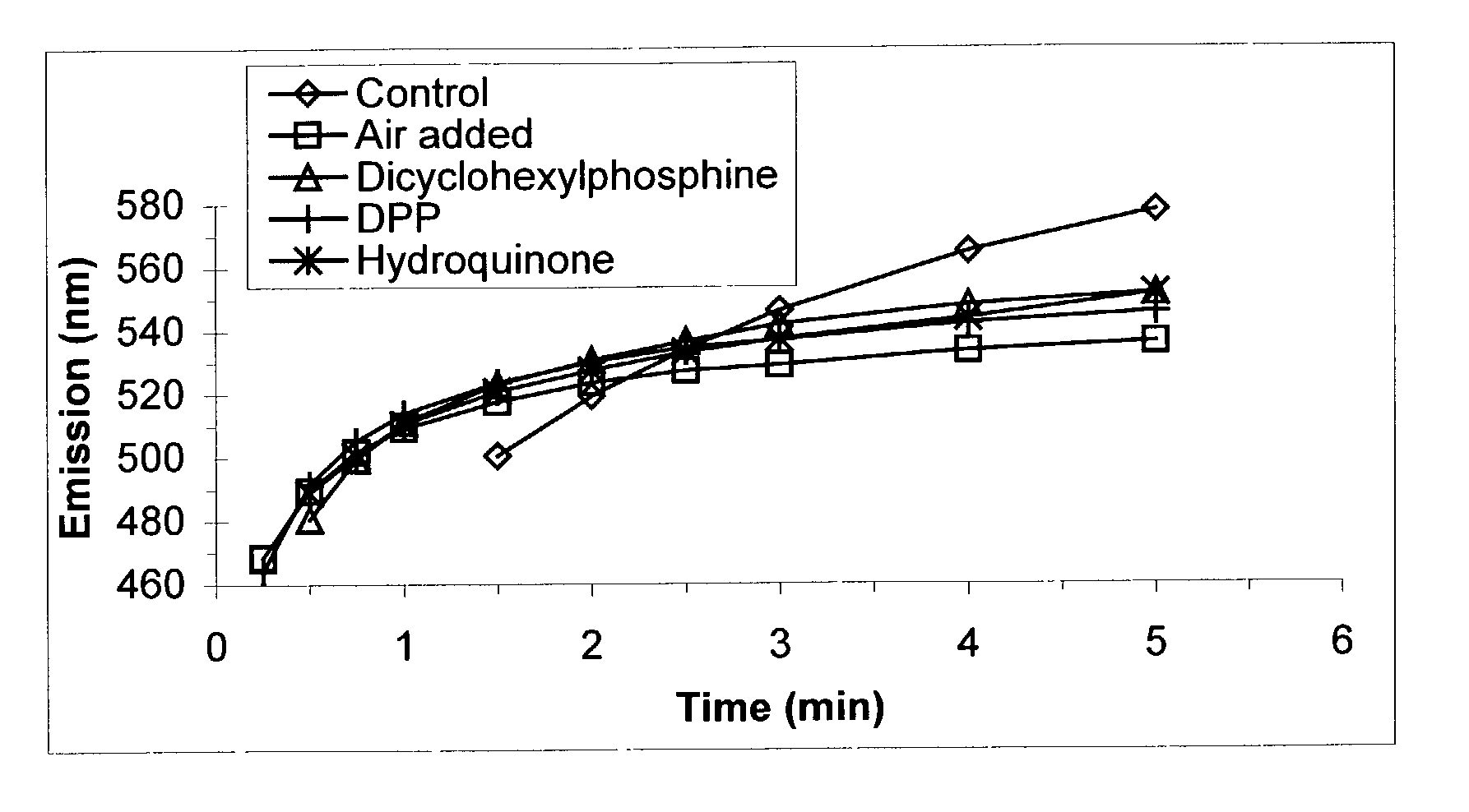
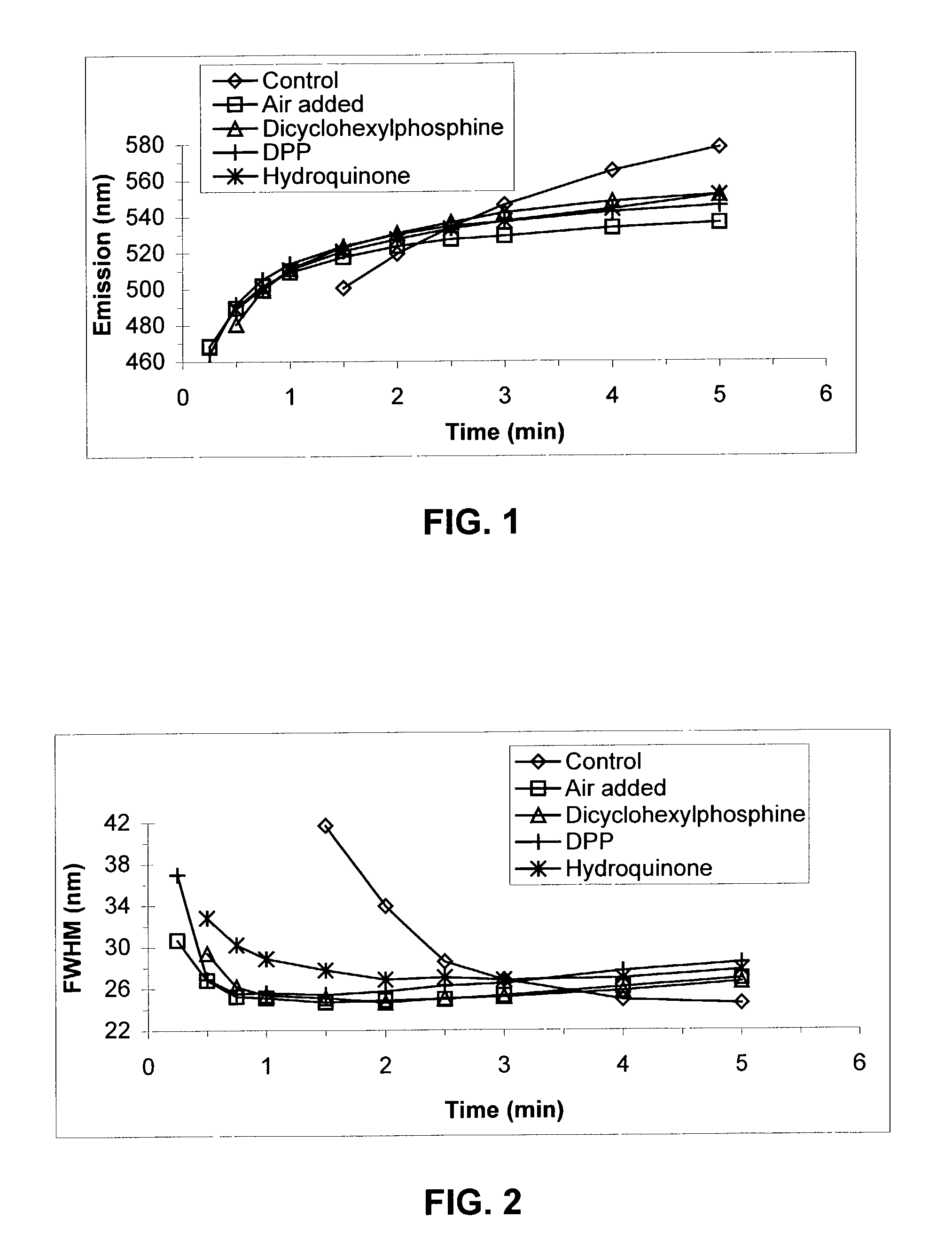
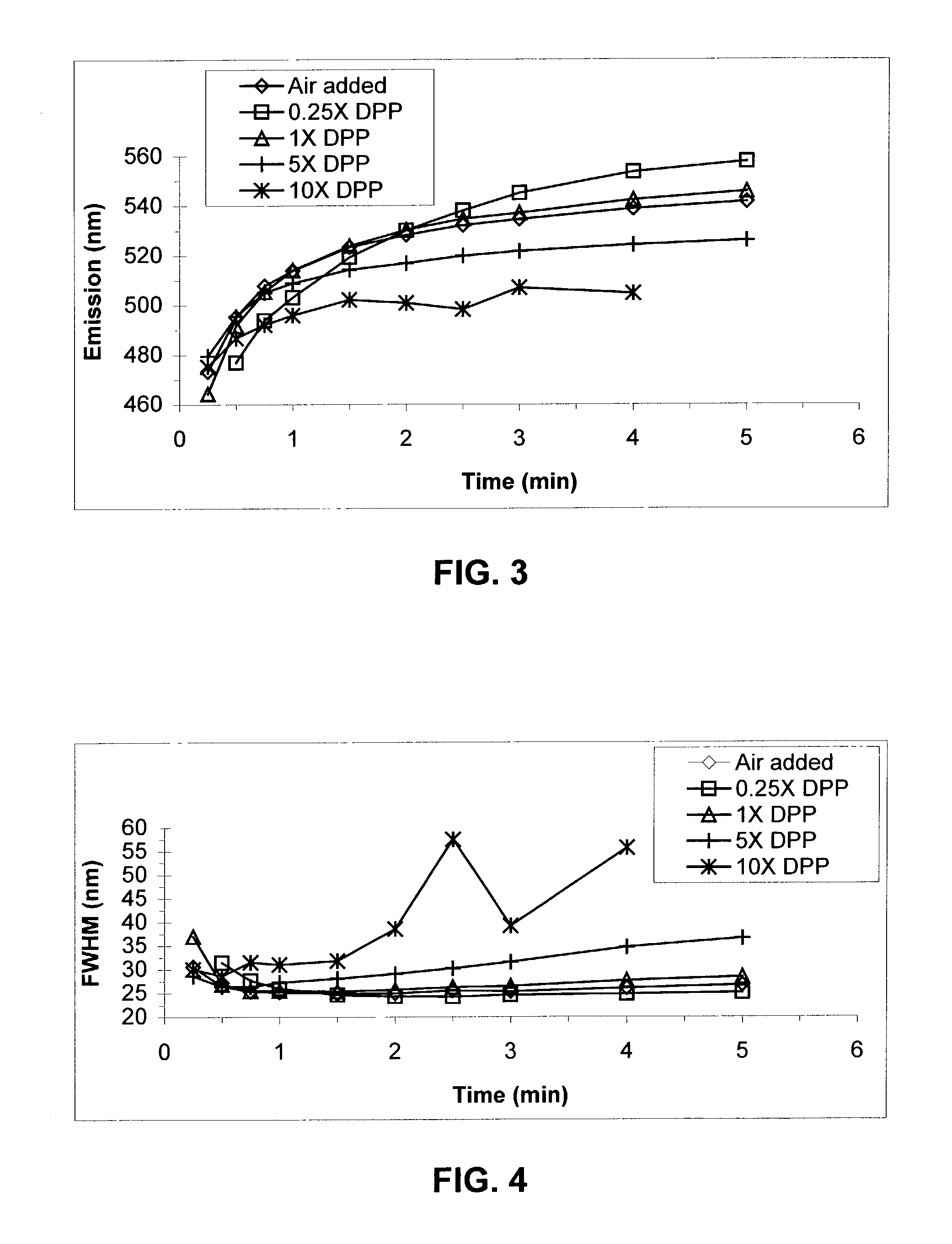
[0111]TOPO (6.0 g) and TDPA (0.577 g) were combined in a three-neck round bottom flask equipped with a stir bar, a thermocouple attached to a temperature controller unit, and a condenser connected to a nitrogen / vacuum manifold. The third neck was sealed with a septum. The atmosphere inside the reactor was evacuated once and refilled with dry nitrogen. Inside an inert atmosphere glove box, a cadmium precursor solution (0.5 m) was prepared by combining cadmium acetate (21.6 g) and TOP (166 g) and allowing the mixture to stir for˜24 hours until fully dissolved. An aliquot (2.03 g) of this solution was diluted with TOP (3.6 mL) and injected via syringe into the reaction vessel. A 16-gauge needle was inserted into the septum of the reaction vessel so that the vessel could be continuously flushed with nitrogen for approximately 10 min as the reaction was heated to 250° C. The needle was removed and heating continued to 260° C. Heating was continued at 260–27...

example 2

Reactions with Hydroquinone Added

[0113]These reactions were carried out as described in Example 1, with the following modifications. No phosphine-based reaction promoter was added to these reactions. Instead hydroquinone (0.226 g) was combined with the TOPO and TDPA solids prior to the nitrogen flush of the reactor in the first step.

example 3

Reactions Demonstrating the Use of Air as a Reagent

[0114]In this example, TOP was obtained from Fluka and used as received. A solution of Se was prepared by dissolving Se (3.16 g) in TOP (33.2 g) (TOPSe). Separately, a cadmium precursor stock solution was prepared by dissolving anhydrous cadmium acetate (6.15 g) in TOP to a final volume of 40 mL (cadmium stock solution). In each of three round bottom flasks, TOPO (5.0 g) was combined with cadmium stock solution (1.4 mL), TDPA (0.52 g), and TOP (1.1 mL) and heated to 250° C. while continuously flushing the vessel with N2. Once the temperature reached 250° C., the nitrogen flush was halted and the temperature was increased to 270° C. This temperature was maintained for 20 min and the solutions were cooled to 100° C. Using a large-bore needle, dry air was directed into each of two flasks at a rate of 200 ml / min for a duration of 1 minute or 10 minutes. A third flask received dry nitrogen for 10 minutes at the same flow rate. Stirring o...


PUM

PropertyMeasurementUnit
emission peak wavelengthaaaaaaaaaa

Abstract

A method is described for the manufacture of semiconductor nanoparticles. Improved yields are obtained by use of a reducing agent or oxygen reaction promoter.

Description

CROSS REFERENCE TO RELATED APPLICATIONS[0001]This application claims priority under 35 U.S.C. § 119(e)(1) to U.S. Provisional Application Ser. No. 60 / 326,746, filed Oct. 2, 2001; U.S. Provisional Application Ser. No. 60 / 401,671, filed Aug. 6, 2002; and U.S. Provisional Application Ser. No. 60 / 404,628, filed Aug. 19, 2002; the disclosures of which are incorporated by reference herein in their entireties.FIELD OF THE INVENTION[0002]This invention relates to nanoparticles. More particularly, the invention relates to methods for making and using semiconductor nanoparticles. The invention finds utility in a variety of fields, including biology, analytical and combinatorial chemistry, medical diagnostics, and genetic analysis.BACKGROUND OF THE INVENTION[0003]Semiconductor nanocrystals (also known as quantum dot particles) whose radii are smaller than the bulk exciton Bohr radius constitute a class of materials intermediate between molecular and bulk forms of matter. Quantum confinement of...

Claims


Application Information

Patent Timeline
Patent Type & Authority Patents(United States)
IPC IPC(8): C30B7/00B82B3/00C01B19/04C30B21/02C30B28/06H01L21/00
CPCB82Y30/00C01B19/007C30B7/14C30B29/48C30B29/60C30B7/00C01P2004/64
Inventor ZEHNDER, DONALD A.TREADWAY, JOSEPH A.
Owner INVITROGEN
Learn More