
Method for forming a fragile layer inside of a single crystalline substrate preferably for making silicon-on-insulator wafers

Inactive Publication Date: 2006-12-12
USENKO ALEXANDER YURI
View PDF6 Cites 126 Cited by
  • Summary
  • Abstract
  • Description
  • Claims
  • Application Information

AI Technical Summary

Benefits of technology

[0024]It is an object of the present invention to provide an inexpensive process for creation of fragile layer inside of a single crystalline substrate. The fragile layer enables further cleavage of the wafer along the layer.

Problems solved by technology

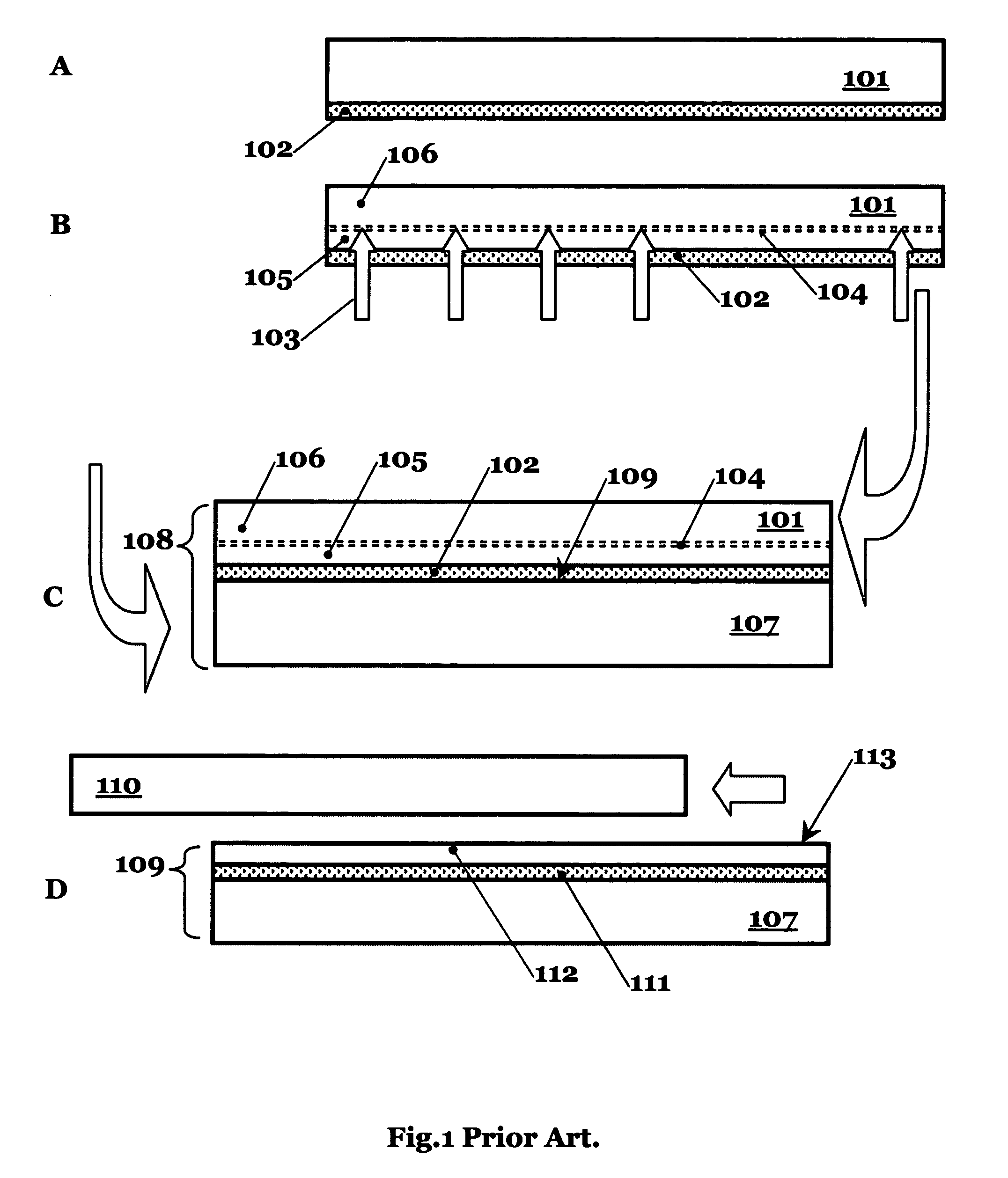
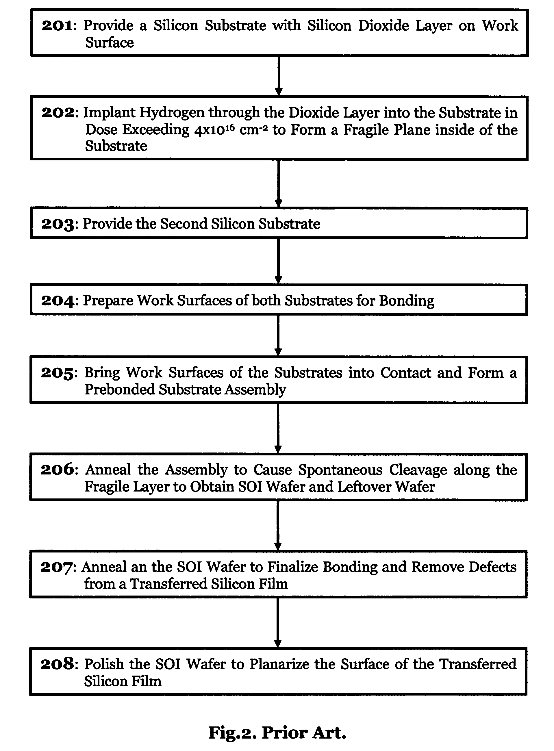
The most important drawbacks of the Smart-Cut are as follows:(1) difficult to get thin transferred layer;(2) high manufacturing cost.
The difficulty in the transfer of thinner layers in the Smart-Cut is caused by the use of hydrogen implantation into plain silicon lattice.
Chip manufacturing, however, requires much thinner superficial silicon, and insulator layer thicknesses.
Smart-cut however, is limited to layer transfers in excess of 200 nm.
At lower energies, Smart-Cut process fails.
This results in quite narrow peak of distribution of high energy ions.
The diffused profile causes the Smart-Cur failure.
Another reason why Smart-Cut fails to transfer thin films relates to surface damage by sub-20 keV ions.
Without bonding, the layer cannot be transferred, and Smart-Cut fails.
Another cause why Smart-Cut fails to transfer thin films is a premature blistering of wafer surface if the wafer is implanted with low energy ions.
Low energy implantation results in shallow location of the bubbles.
Thinning however increases thickness non-uniformity of the superficial crystalline film of SOI wafer that is highly undesirable.
High manufacturing costs of the Smart-Cut are caused by necessity of prolonged hydrogen implanting.
Hydrogen implantation in Smart-Cut cannot however benefit from high ion beam current.
If the target (i.e, silicon wafer) is heated over about 80° C. during the implantation, Smart-Cut fails.
Heating of the wafer under implantation causes premature blistering.
Therefore the best achievable throughput in the Smart-Cut is limited to about 10 wph (wafers per hour).
This is not enough to achieve a cost-efficient SOI wafer production.
The direct replacement of the beam implantation by plasma immersion in the Smart-Cut results, however, in much worse quality of final SOI wafers.
A crystalline quality of that heavily hydrogenated silicon cannot be healed by annealing to a level required by chip production.
Some of them works as infinite traps for hydrogen; and the higher dose hydrogen implantation, the bigger amount of hydrogen platelets and bubbles will be created on these unintentional and unavoidable traps.
The hydrogen platelets and the bubbles are non-point defects, and silicon that contains these features cannot be annealed to restore its initial perfect lattice.
Finally, plasma immersion implantation version of the Smart-Cut results in SOI wafers with low quality superficial silicon.
Another problem with Henley's process is that it results in thinner transferred layers at wafer periphery as compared to the wafer center.
Fan et al. in Z. Fan, P. K. Chu, N. W. Cheung, C. Chan, Thickness uniformity of silicon-on-insulator fabricated by plasma immersion ion implantation and ion cut, IEEE Transactions on Plasma Science, Vol. 27, 1999, pages 633–636 given an experimental evidence of thickness non-uniformity of the plasma immersion implantation version of the Smart-Cut; the thickness non-uniformity is a serious quality problem in the final SOI wafer.
These Smart-Cut improvements either partially resolve the thickness and cost related Smart-Cut issues, or create quality issues.
Agarwal's approach, however, does not solve the thickness problems of the Smart-Cut.
Subsequently, the thickness limitation is the same as in the Smart-Cut, and thin transfers are not enabled by Goesele.
Therefore the throughput problem is not solved by Goesele either.
We believe that Bower's process cannot enable the ultrathin transfers.
Due to Bower's teaching, annealing of the boron-implanted wafer result in complete removal of implantation damages and in electrical activation of boron.
This says that sub-100-nm layer transfers will be extremely non-uniform in thickness, and thus are not technically featurable for thin SOI production.
Another reason, why Bower's teaching cannot be applied for manufacturing of thin SOI relates to unwanted altering of electrical properties of the transferred silicon layer.
Chips cannot be manufactured in these heavy doped films for several reasons, for example, because carrier mobility drastically drops in heavy doped semiconductors, and also because a depleted zone will not extend through entire thickness of silicon film, so fully depleted devices cannot be manufactured.
This process is free from limitations inherent to Smart-Cut cut process as relative to thickness and to implant-related cost, but it is more difficult to get high quality SOI wafers using the U.S. Pat. No. 6,352,909 process.
The quality problems appear in both, electrolytic, and plasma methods of hydrogenation.
The etching preferentially proceeds on defected surface areas, therefore the etching is not area-uniform, and roughness of silicon wafer surface increases.
The rough surface wafer is difficult to bond to a destination wafer.
The roughness causes bonding voids between the wafers.
The voids cause layer transfer faults, and a final SOI wafer has areas with missing superficial silicon.
These wafers are rejected and are not useful anymore.

Method used


Image

  • Method for forming a fragile layer inside of a single crystalline substrate preferably for making silicon-on-insulator wafers
  • Method for forming a fragile layer inside of a single crystalline substrate preferably for making silicon-on-insulator wafers
  • Method for forming a fragile layer inside of a single crystalline substrate preferably for making silicon-on-insulator wafers

Examples


Embodiment Construction

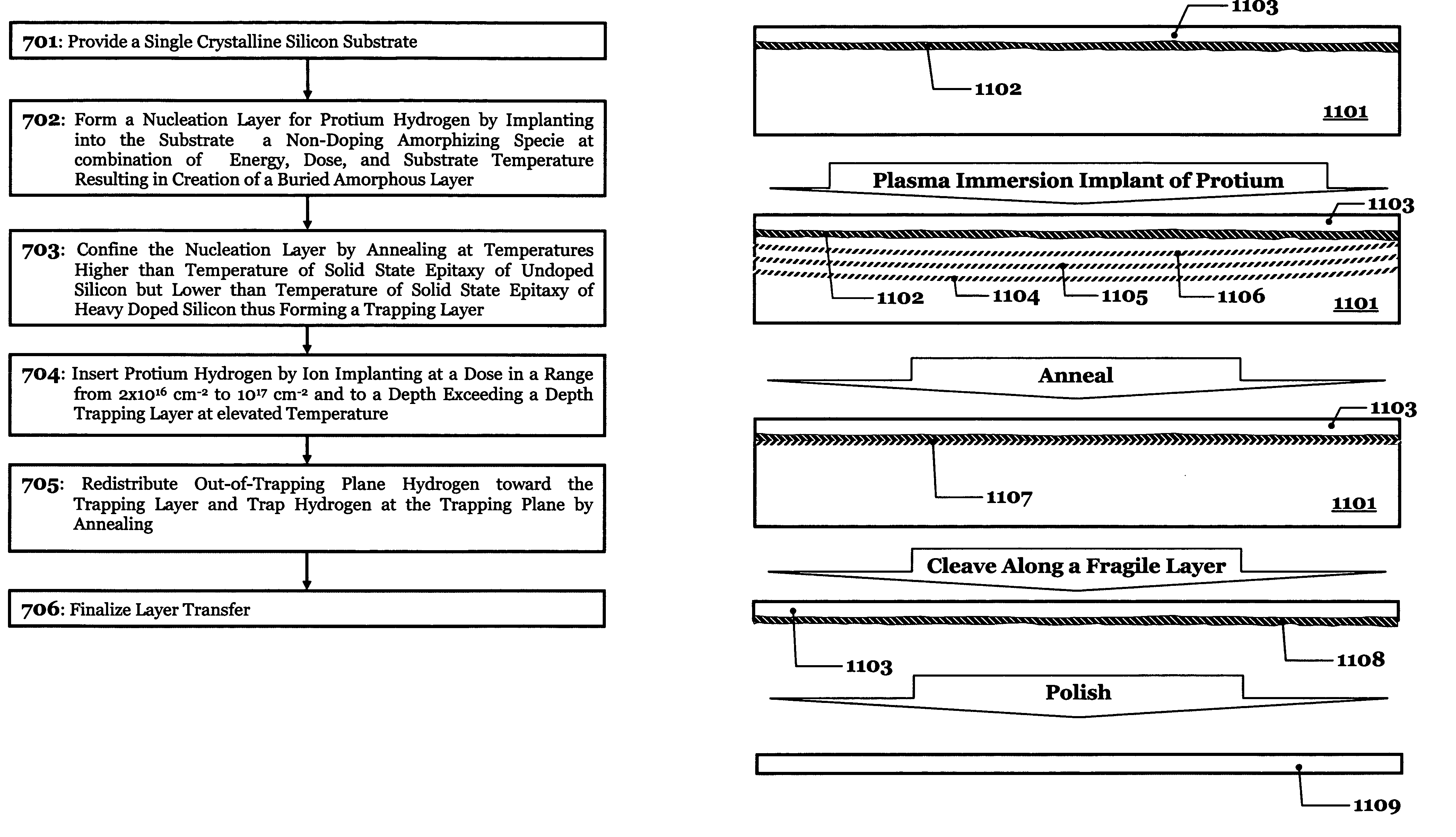
[0056]The invention is illustrated by three preferred embodiments:[0057](1) using of deuterium implantation for creation of a trapping layer[0058](2) using of an amorphizing implantation for creation of a trapping layer[0059](3) using plasma immersion ion implantation of protium into a denuded wafer.

[0060]It is to be understood that the described embodiments are merely illustrative of the invention and that many variations may be devised by those skilled in the art without departing from the scope of the invention and from the principles disclosed herein. It is therefore intended that such variations be included within the scope of the following claims and their equivalents.

DETAILED DESCRIPTION OF THE FIRST PREFERRED EMBODIMENT

[0061]This embodiment allows one to fabricate SOI wafers with high throughput.

[0062]An embodiment, which will now be described, shows a method for making an SOI wafer with a deuterium implantation for creating a nucleation (trapping) layer for hydrogen and pro...


PUM


Abstract

Process for forming a fragile layer inside of a single crystalline substrate near one of the substrate surfaces. The fragile layer is created by collecting hydrogen in high concentration at a desired depth. The hydrogen layer is collected on a seed layer. The seed layer is formed by ion implantation of non-doping species and annealing. The implantation introduces defects that are capable to trap hydrogen, and annealing confines the seed layer making it flat and thin. Then protium hydrogen ions are implanted at elevated temperature. The protium implantation depth is bigger than the depth of the seed layer. The implanted protium moves to the seed layer and trap there. The process is useful for making silicon-on-insulator (SOI) wafers. SOI with an ultrathin superficial silicon layer of high quality can be obtained. Hydrogen can be implanted at high dose rate, and thus the SOI wafers can be manufactured with high throughput and low cost. SOI wafers also have high quality as superficial silicon does not contain microvoids.

Description

FIELD OF THE INVENTION[0001]The present invention relates generally to a fabrication of silicon-on-insulator (SOI) wafers. More particularly the present invention relates to a cost efficient process of making a fragile plane inside of a single crystalline silicon wafer at shallow depth under the wafer surface.BACKGROUND OF THE INVENTION[0002]Silicon-on-insulator (SOI) wafer is a starting material for making advanced semiconductor chips. Currently the most advanced method of making the SOI wafers is a layer transfer method. In the layer transfer method, a thin film of crystalline material is delaminated from a first wafer and laminated on a surface of a second wafer. The first wafer is called a donor wafer, and the second one is called a destination wafer. Either the donor or the destination wafer or both can have insulating films on their surfaces. Those insulator films further appear as a middle layer in a 3-layer sandwich structure that is obtained by the layer transfer process. T...

Claims


Application Information

Patent Timeline
IPC IPC(8): H01L21/76
CPCH01L21/76254
Inventor USENKO, ALEXANDER YURI
Owner USENKO ALEXANDER YURI
Learn More