Semiconductor integrated circuit

a technology of integrated circuits and semiconductors, applied in the field of semiconductor integrated circuits, to achieve the effects of preventing data retention loss, efficient operation of refresh timers, and reducing standby curren

Active Publication Date: 2006-12-12
SOCIONEXT INC
View PDF13 Cites 34 Cited by
  • Summary
  • Abstract
  • Description
  • Claims
  • Application Information

AI Technical Summary

Benefits of technology

[0011]It is an object of the present invention to reduce current consumption of a semiconductor integrated circuit having a temperature detector.
[0012]It is another object of the present invention to prevent malfunction of a temperature detector due to noises, thereby preventing malfunction of a semiconductor integrated circuit.

Problems solved by technology

Further, since the first boundary temperature and the second boundary temperature set a buffer zone, the temperature detector does not detect power supply noises or the like generated due to the operation of internal circuits as temperature variation.

Method used


Image

  • Semiconductor integrated circuit
  • Semiconductor integrated circuit
  • Semiconductor integrated circuit

Examples


first embodiment

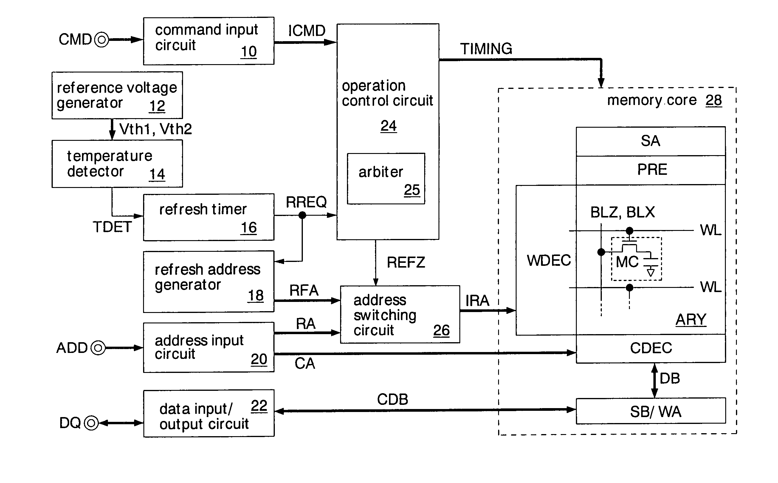
[0062]FIG. 4 shows the semiconductor integrated circuit of the present invention. This semiconductor integrated circuit is formed on a silicon substrate as a pseudo SRAM, using a CMOS process. The pseudo SRAM has a memory core of a DRAM and an interface of an SRAM. The pseudo SRAM executes a refresh operation periodically inside a chip without receiving an external refresh command and retains data written to memory cells. The pseudo SRAM is used as a work memory mounted on, for example, a cellular phone. A read operation and a write operation are executed in response to command signals CMD (a read command signal and a write command signal) supplied via an external terminal.

[0063]The pseudo SRAM has a command input circuit 10, a reference voltage generator 12, a temperature detector 14, a refresh timer 16, a refresh address generator 18, an address input circuit 20, a data input / output circuit 22, an operation control circuit 24, an address switching circuit 26, and a memory core 28....

second embodiment

[0106]The reference voltage setting circuit 42 outputs 8-bit setting signals SET in order to initially set respective values of the threshold voltages Vth1–4 to be generated by the reference voltage generator 36. 2 bits of the setting signals SET are used to make the initial setting of each of the threshold voltages Vth1–4. The logic of the setting signals SET is fixed during manufacturing processes of the pseudo SRAM as in the

[0107]FIG. 13 shows the temperature detector 38 shown in FIG. 12 in detail. A temperature detecting unit 14a, differential amplifiers 14b, 14c, and a flipflop 14d for generating the temperature detecting signal TDET1 are the same as those in the temperature detector 14 (FIG. 5) of the first embodiment. Further, the temperature detector 38 has differential amplifiers 38b, 38c and a flipflop 38d for generating the temperature detecting signal TDET2.

[0108]An output (a detection voltage N31) of the temperature detecting unit 14a is inputted in common to the differ...

sixth embodiment

[0137]The reference voltage generator 58 has a resistor array 54e in place of the resistor array 54d of the The other configuration is the same as the logical configuration of the reference voltage generator 54 of the six embodiment. The resistor array 54e has four resistors connected in series. A threshold voltage Vth1 (or Vth2, Vth3, Vth4) is generated from a connecting node of two adjacent resistors.

[0138]The same effects as those of the above-described first, second, fourth, and sixth embodiments are also obtainable in this embodiment.

[0139]FIG. 20 shows an eighth embodiment of the semiconductor integrated circuit of the present invention. The same reference numerals and symbols are used to designate the same elements as the elements explained in the first and fifth embodiments, and detailed explanation thereof will be omitted. The semiconductor integrated circuit of this embodiment is formed on a silicon substrate as a DRAM having a self-refresh function, using a CMOS process....


PUM

PropertyMeasurementUnit
temperatureaaaaaaaaaa
boundary temperatureaaaaaaaaaa
detection voltageaaaaaaaaaa

Abstract

A temperature detector sets the level of a temperature detecting signal to a level indicating a high temperature state, detecting that the chip temperature is higher than a first boundary temperature. The temperature detector sets the level of thereof to a level indicating a low temperature state, detecting that the chip temperature is lower than a second boundary temperature. A control circuit changes its operating state according to the level of the temperature detecting signal. This prevents the operating state of the control circuit from frequently switched even when the chip temperature fluctuates around the boundary temperatures, and accordingly reduces current consumption of the control circuit due to the switching operation. Further, the first and second boundary temperatures set a buffer zone, so that the temperature detector does not detect power supply noises as temperature variation. This can prevent malfunction of the temperature detector and the semiconductor integrated circuit.

Description

CROSS REFERENCE TO RELATED APPLICATION[0001]This application is based upon and claims the benefit of priority from Japanese Patent Application No. 2003-375276, filed on Nov. 5, 2003 and No. 2004-187938, filed on Jun. 25, 2004, the entire contents of which are incorporated herein by reference.BACKGROUND OF THE INVENTION[0002]1. Field of the Invention[0003]The present invention relates to a semiconductor integrated circuit having a temperature detector.[0004]2. Description of the Related Art[0005]An SRAM has been conventionally used as a work memory of portable equipment such as a cellular phone. However, memory capacity necessary for portable equipment has been increasing year after year. Therefore, a DRAM having dynamic memory cells or a pseudo SRAM is adopted as a work memory in recent years. A DRAM can have larger memory capacity as a work memory with the same cost since a memory cell thereof is smaller than a memory cell of the SRAM.[0006]Meanwhile, a memory mounted on a cellular...

Claims


Application Information

Patent Timeline
Patent Type & Authority Patents(United States)
IPC IPC(8): G01K1/00H03K17/94G01K7/00G11C11/403G11C11/406
CPCG01K7/00G11C11/406G11C11/40615G11C11/40626G11C2211/4067
Inventor KOBAYASHI, HIROYUKISAKO, ATSUMASA
Owner SOCIONEXT INC
Why Eureka
Try Eureka