Contact probe, method of manufacturing the contact probe, and device and method for inspection

a technology of contact probe and manufacturing method, which is applied in the direction of contact probe manufacturing, semiconductor/solid-state device testing/measurement, instruments, etc., can solve the problems of point contact not being achieved, contact pressure not being increased above a prescribed level, and the contact probe itself being weaker, etc., to achieve reliable conduction, reliable conduction, and reliable conduction

Inactive Publication Date: 2006-12-19
SUMITOMO ELECTRIC IND LTD
View PDF24 Cites 19 Cited by
  • Summary
  • Abstract
  • Description
  • Claims
  • Application Information

AI Technical Summary

Benefits of technology

[0012]In order to achieve the aforementioned object, based on the first invention, a contact probe having a tip end portion, is formed of an electroforming metal layer grown in a direction in accordance with a certain pattern. The tip end portion is sharpened by being provided with a slope formed by machining that intersects obliquely with respect to a growing direction of the electroforming. By employing such a configuration, a sharpened tip end portion attains point contact with an object of measurement, rather than linear contact, thereby increasing a contact pressure.
[0028]In the test method, preferably, the contact probe is manufactured by performing lithography and electroforming. Specifically, a contact probe that is manufactured by lithography and electroforming is often used for a test of a high-density, fine circuit and then confronts the existence of the oxide film. On the contrary, in the present invention, since a test is performed while the oxide film is being removed in the reduction gas environment, more reliable conduction is provided and a precise test can be performed effectively. Although a nozzle may be arranged beside each contact probe to blow the reduction gas, it is difficult in a test of a high-density, fine circuit to install a nozzle in a limited area in which a contact probe may be arranged. Therefore, it is more preferable to eliminate the. need for a nozzle for each contact probe by placing the test environment itself in the reduction gas, rather than to install a nozzle for blowing the reduction gas. In this test method, it is unnecessary to install a nozzle, and therefore the density of contact probes can be increased.

Problems solved by technology

In other words, point contact cannot be achieved and therefore the contact pressure cannot be increased above a prescribed level.
Furthermore, while the contact pressure has to be increased to some extent in order to break through the insulating film, the finer the contact probe becomes, the weaker the contact probe itself becomes, making it difficult to increase a load.
Moreover, application of a high pressure is also unfavorable for the substrate under test.
Such a method, however, requires a combination of multiple components, which would complicates the structure, thereby making miniaturization difficult and also increasing the cost, inevitably.
Therefore, the probe has to be brought into contact under an excessively high contact pressure to break through the insulating film, and additional shaping process is required to obtain a needle-like tip end.

Method used


Image

  • Contact probe, method of manufacturing the contact probe, and device and method for inspection
  • Contact probe, method of manufacturing the contact probe, and device and method for inspection
  • Contact probe, method of manufacturing the contact probe, and device and method for inspection

Examples


first embodiment

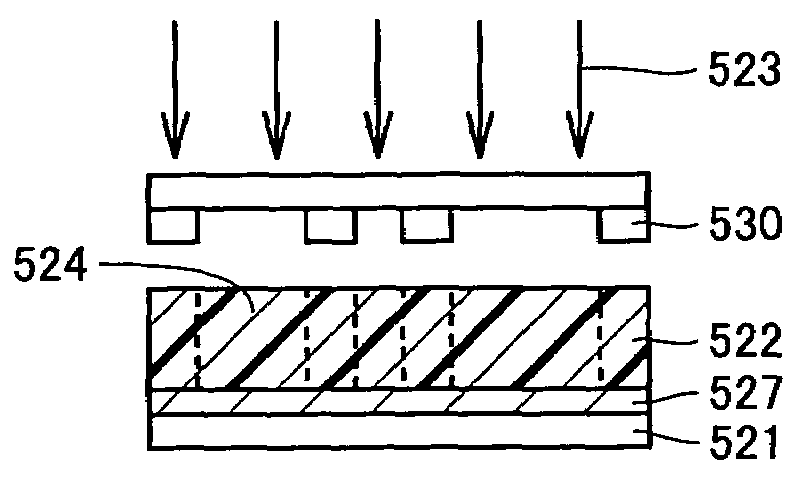
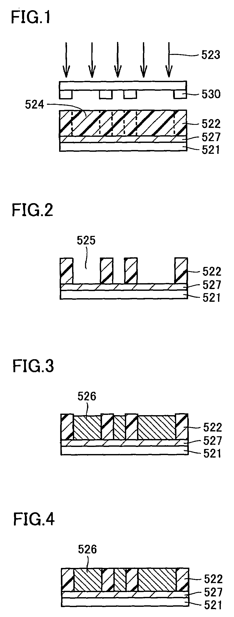
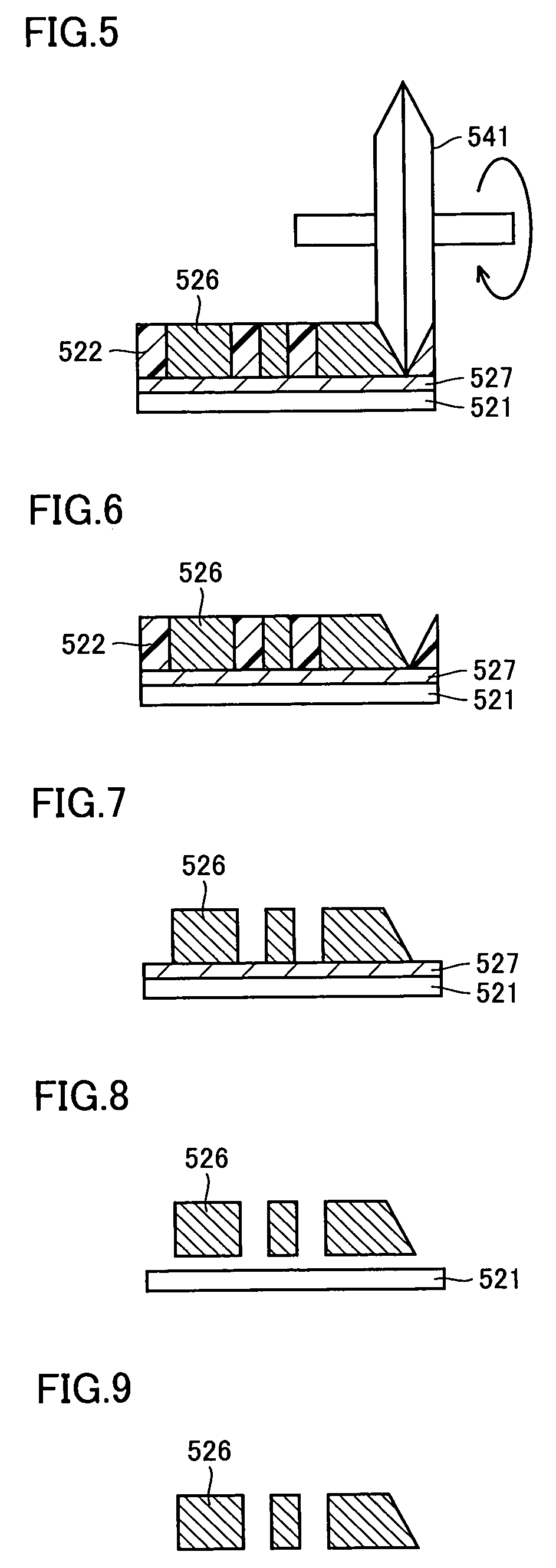
[0070]Referring to FIGS. 1–9, a method of manufacturing a contact probe of a first embodiment based on the first invention will be described.

[0071]First, a resist film 522 is formed on an upper surface of a conductive substrate 521. A metal substrate including SUS, Cu, Al, or the like, an Si substrate, a glass substrate, or the like can be used as substrate 521. It is noted that in the case of an Si substrate, a glass substrate, or the like, a metal layer of Ti, Al, Cu, Ni, Mo, or a combination thereof is formed in advance on the upper surface of substrate 521 by sputtering to serve as an underlying conductive layer 527. Alternatively, even in the case of using a metal substrate, the underlying conductive layer may be formed by sputtering or the like on the metal substrate as necessary. In the following, description will be made with reference to the figures, assuming that underlying conductive layer 527 is present.

[0072]As shown in FIG. 1, using a mask 530, the surface of resist fi...

second embodiment

[0081]Referring to FIGS. 13–21, 8 and 9, a method of manufacturing a contact probe in a second embodiment based on the first invention will be described.

[0082]As shown in FIG. 13, using a metal die 532 having convexity as the shape of the contact probe, a resin die 533 is formed by injection molding. As a result, a resin die 533 having concavity as the shape of the contact probe results. This resin die 533 is polished so that the concave portion is penetrated in order to fabricate a resin pattern frame 534 as shown in FIG. 15. As shown in FIG. 16, substrate 521 having underlying conductive layer 527 formed on the upper surface thereof is prepared, as in the first embodiment, and resin pattern frame 534 is affixed on the upper surface thereof. As described in the first embodiment, underlying conductive layer 527 may be omitted if substrate 521 is a metal substrate. The concave portion may be penetrated after resin die 533 is affixed to substrate 521 (not shown). As shown in FIG. 17, ...

third embodiment

[0086]Referring to FIGS. 1–4, 22, 23, and 7–9, a method of manufacturing a contact probe in a third embodiment based on the first invention will be described.

[0087]The steps shown in FIGS. 1–4 are the same as described in the first embodiment. As shown in FIG. 4, the upper surface of metal layer 526 is ground or polished to attain a uniform thickness as desired, in the present embodiment, followed by ashing to remove resist film 522, as shown in FIG. 22. As shown in FIG. 23, electrical discharge machining is performed using an electrical discharge machining electrode 542. Electrical discharge machining electrode 542 is an electrode having a tip end formed into a conical shape or a V-shape. In this electrical discharge machining, a machined surface is formed obliquely with respect to the part serving as the tip end portion of the contact probe.

[0088]In the example shown in FIG. 23, electrical discharge machining is performed with metal layer 526 being affixed on substrate 521, althou...


PUM

PropertyMeasurementUnit
thicknessaaaaaaaaaa
lengthaaaaaaaaaa
thicknessaaaaaaaaaa

Abstract

A method of manufacturing a contact probe includes an electroforming step of, using a resist film (522) arranged on a substrate (521) as a pattern frame having a shape corresponding to a contact probe, performing electroforming to fill a gap in the resist film (522) to form a metal layer (526), a tip end shaping step of obliquely removing and sharpening that part of the metal layer (526) which serves as a tip end portion of the contact probe, and a take-out step of taking out only the metal layer (526) from the pattern frame.

Description

RELATED APPLICATION DATA[0001]This application is a national stage 371 of PCT / JP02 / 00444 filed Jan. 22, 2002.TECHNICAL FIELD[0002]The present invention relates to a contact probe for use with a test apparatus for performing an electrical test of a circuit under test such as a semiconductor substrate and a liquid crystal display, and a method of manufacturing the same. The present invention also relates to a test apparatus and a test method.BACKGROUND ART[0003]A test of a circuit formed on a semiconductor substrate or a liquid crystal display is generally performed using a test apparatus with an electrode portion (which is called, for example, a probe card) having a number of contacts (or contact needles) called contact probes being arranged correspondingly to a circuit pattern to be tested. Miniaturization of contact probes has been required, and as disclosed in Japanese Patent Laying-Open No. 2000-162241, for example, it is possible to manufacture a ultra-fine contact probe having ...

Claims


Application Information

Patent Timeline
Patent Type & Authority Patents(United States)
IPC IPC(8): G01R31/02H01K3/10G01R1/067G01R3/00G01R15/24
CPCG01R1/06733G01R1/06738Y10T29/49117G01R3/00Y10T29/49204G01R1/06755H01L22/00
Inventor HIRATA, YOSHIHIROHAGA, TSUYOSHINUMAZAWA, TOSHIYUKINAKAMAE, KAZUOOKADA, KAZUNORIYORITA, JUN
Owner SUMITOMO ELECTRIC IND LTD
Why Eureka
Try Eureka