Surface acoustic wave device and method for manufacturing same

a surface acoustic wave and acoustic wave technology, applied in the direction of generators/motors, instruments, impedence networks, etc., can solve the problems of reducing the efficiency of manufacturing, and causing a large amount of plastic strain and creep strain, so as to achieve the effect of drastically improving the manufacturing efficiency

Active Publication Date: 2006-12-26
KYOCERA CORP
View PDF5 Cites 33 Cited by
  • Summary
  • Abstract
  • Description
  • Claims
  • Application Information

AI Technical Summary

Benefits of technology

[0024]Because of the use of a Sn—Sb based lead-free solder containing 90% or more Sn for the solder bump component and solder sealing component, metal fatigue caused by thermal stress due to the difference in thermal expansion coefficient is reduced, so that stable connection is maintained for a long duration of time as compared with conventional cases where solders containing lead are used for the joining.
[0048]Also, the arrangement may be such that a large-size base substrate comprising a plurality of base substrates formed with the electrode for connection to the element and the periphery sealing conductor film is prepared, surface acoustic wave elements are joined to the respective base substrate sections, and the large-size base substrate is cut to be separated into individual base substrate sections. As a result, a plurality of devices can be substantially collectively manufactured, so that the manufacturing efficiency can be drastically improved.

Problems solved by technology

However, since lead-containing solders used for joining components contribute to deterioration of the environment, the use thereof is to be restricted.
In addition, because of the weak yield stress of the solder materials containing great amounts of lead, when thermal stress is generated due to the difference in thermal expansion coefficient between the surface acoustic wave element and the substrate, great amounts of plastic strain and creep strain are caused.
However, when they are subjected to a temperature cycle test assuming an actual long duration of use, stress due to the difference in thermal expansion coefficient between the surface acoustic wave element and the base substrate acts intensely on the solder joint.
The stress repeatedly acts on the solder joint causing metal fatigue in that section, finally breaking the joint.
In addition, in the foregoing surface acoustic wave device, since heat from the solder reflow or the like also propagates to the interior of the surface acoustic wave device when it is mounted on the motherboard, the soldering material that joins the surface acoustic wave element and the base substrate together is also subjected to heat.
As a result, short circuit would occur in the connector electrode of the surface acoustic wave element.
In addition, due to the use of a pyroelectric component for the surface acoustic wave element of the surface acoustic wave device, sparks are generated during the reflow treatment between electrode fingers of the comb-shaped IDT electrode engaged with one another on the piezoelectric substrate, causing pyroelectric breakdown to occur in the IDT electrode.
The generation of sparks becomes prominent when the speed of temperature increase during the reflow treatment is high.
However, in this way, the reflow treatment takes too long time, which makes it difficult to manufacture surface acoustic wave devices with high efficiency.
This is because misalignment cannot be corrected after the base substrate and the surface acoustic wave device are introduced into the chamber because of the nitrogen atmosphere of the chamber.
However, if the reflow treatment is carried out in such a condition, the flux component scatters inside the gap surrounded by the solder sealing component and adheres to the surface of the surface acoustic wave element, leading to deterioration of the properties.
For this reason, even if the pressure inside the chamber is reduced to bring the chamber into a nitrogen atmosphere, it is difficult to reliably bring the gap region formed between the surface acoustic wave element and the base substrate into a nitrogen atmosphere.

Method used


Image

  • Surface acoustic wave device and method for manufacturing same
  • Surface acoustic wave device and method for manufacturing same
  • Surface acoustic wave device and method for manufacturing same

Examples


Embodiment Construction

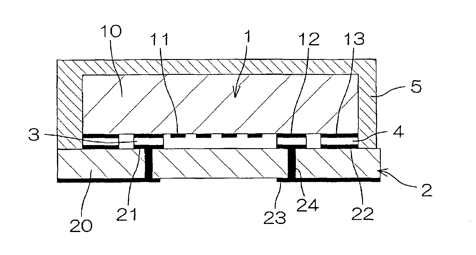
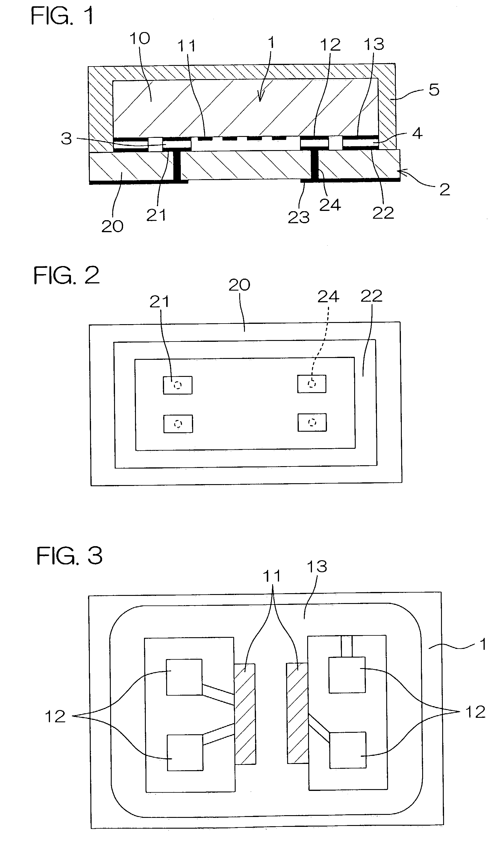
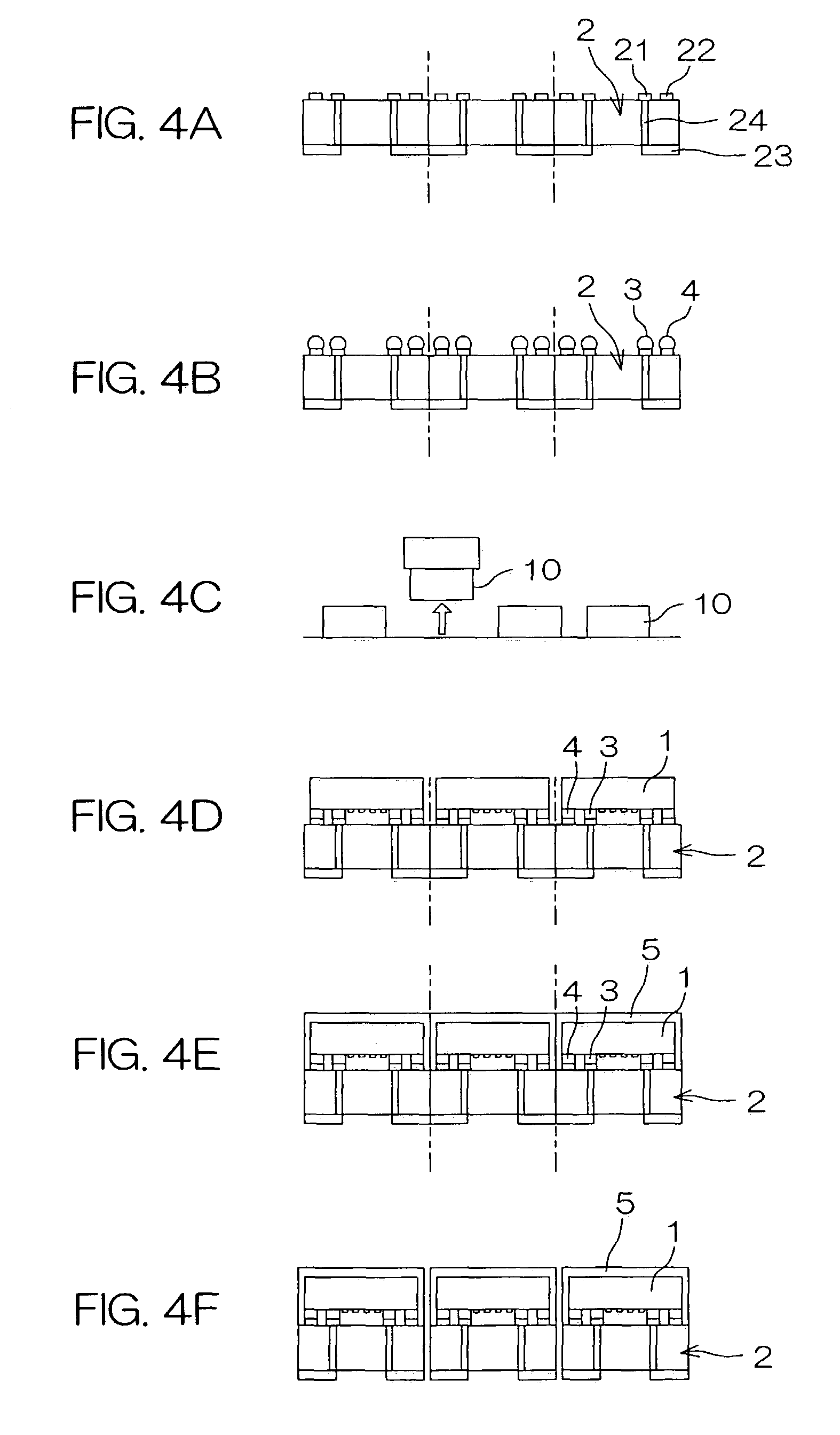
[0073]FIG. 1 is a cross-sectional view of a surface acoustic wave device according to the present invention and FIG. 2 is a schematic plan view of a base substrate used for the surface acoustic wave device of the present invention. FIG. 3 is a schematic plan view showing various electrodes formed on one principal surface of a surface acoustic wave element.

[0074]The surface acoustic wave device comprises a surface acoustic wave element 1, a base substrate 2, a solder bump component 3, a solder sealing component 4 and an outer covering resin layer 5.

[0075]A surface acoustic wave resonator, surface acoustic wave filter or the like may be quoted as an example of the surface acoustic wave element 1. Each of them comprises a piezoelectric substrate 10 composed of quartz, lithium niobate (LiNbO3), lithium tantalate (LiTaO3) or the like, an Inter Digital Transducer electrode (including a comb-shaped electrode and reflector electrode, which is hereinafter simply referred to as the “IDT elect...


PUM

PropertyMeasurementUnit
elastic modulusaaaaaaaaaa
temperaturesaaaaaaaaaa

Abstract

A surface acoustic wave device is disclosed, which comprises a surface acoustic wave element including a lithium tantalate piezoelectric substrate 10 with one principal surface thereof formed with an IDT electrode 11, a connector electrode 12 and a periphery sealing electrode 13, and a base substrate 2 formed with an electrode 21 for connection to the element connected to the connector electrode 12 through a solder bump component 3 and a periphery sealing conductor film 22 joined to the periphery sealing electrode 13 thorough a solder sealing component 4. For the solder bump component 3 and the solder sealing component 4, a Sn—Sb based or Sn—Ag based lead-free solder containing 90% or more Sn is used, and the thermal expansion coefficient of the base substrate 2 is set in the range of 9–20 pm / ° C. The joining is accomplished with high stability resisting thermal stress due to a difference in thermal expansion coefficient, so that a surface acoustic wave device that can maintain stable connection for a long duration of time can be provided.

Description

[0001]This application is based on applications Nos. 2002-222582, 2002-222583, 2002-316788, 2002-316791, 2002-316792, 2003-21101 and 2003-21104 filed in Japan, the content of which is incorporated hereinto by reference.BACKGROUND OF THE INVENTION[0002]1. Field of the Invention[0003]The present invention relates to a surface acoustic wave device which comprises a surface acoustic wave element that is formed with an inter digital transducer electrode (hereinafter referred to as “IDT electrode”), a connector electrode and a periphery sealing electrode and joined to a base substrate through a solder bump component and a solder sealing component, and a method for manufacturing the same.[0004]2. Description of the Related Art[0005]Conventional surface acoustic wave devices include a monocrystal piezoelectric substrate such as a lithium tantalate substrate or a lithium niobate substrate with one principal surface formed with an IDT electrode, in which a connector electrode for providing si...

Claims


Application Information

Patent Timeline
Patent Type & Authority Patents(United States)
IPC IPC(8): H01L41/08G01H3/12H01L21/56H01L21/60H01L23/31H01L27/14H03H3/08H03H9/10H03H9/25
CPCG01H3/12H03H3/08H03H9/059H03H9/1085Y10T29/42H01L23/3135H01L23/315H01L24/81H01L2224/81801H01L2924/09701H01L21/561Y10T29/435H01L2224/16225H01L2224/16227H01L2224/73203Y10T29/49002H01L2924/00012
Inventor SHIMADA, MITSUTAKAYAMAGATA, YOSHIFUMIOTSUKA, KAZUHIROHISATAKA, MASAFUMIOIKAWA, AKIRAKUWAHATA, MICHIHIKOYAMANO, MASARU
Owner KYOCERA CORP
Why Eureka
Try Eureka