Power amplifier module

a technology of power amplifier and module, which is applied in the direction of printed circuit non-printed electric components association, sustainable manufacturing/processing, and final product manufacturing, etc., can solve the problems of difficult to strengthen a reference potential electrode (ground electrode) on the back surface of an upper-side semiconductor chip, affecting the miniaturization of the product, etc., to achieve favorable heat radiation properties, reduce the thickness of the semiconductor module, and minimize the effect of the semiconductor modul

Inactive Publication Date: 2006-12-26
RENESAS TECH CORP
View PDF9 Cites 27 Cited by
  • Summary
  • Abstract
  • Description
  • Claims
  • Application Information

AI Technical Summary

Benefits of technology

[0028]Such a semiconductor module can provide a three-dimensional mounting structure which arranges the second semiconductor chip (upper semiconductor chip) above the first semiconductor chip (lower semiconductor chip) and hence, compared to the structure which arranges the first and the second semiconductor chips on one plane in parallel, it is possible to miniaturize the semiconductor module. At the same time, since the semiconductor module adopts a structure which fixes the lower semiconductor chip to the bottom of the recess formed in the upper surface of the module board, it is possible to reduce a thickness of the semiconductor module by an amount corresponding to a depth of the recess.
[0029]In such a semiconductor module, the lower surface of the lower semiconductor chip is electrically connected to the heat radiation pad which is set to the reference potential (ground) of the l

Problems solved by technology

On the other hand, as shown in Japanese Unexamined Patent Publication 2001-110986, with respect to the structure which arranges the semiconductor chips in parallel, the miniaturization of the product is impeded.
Further, in the laminated mounting struct

Method used


Image

  • Power amplifier module
  • Power amplifier module
  • Power amplifier module

Examples


embodiment 1

(Embodiment 1)

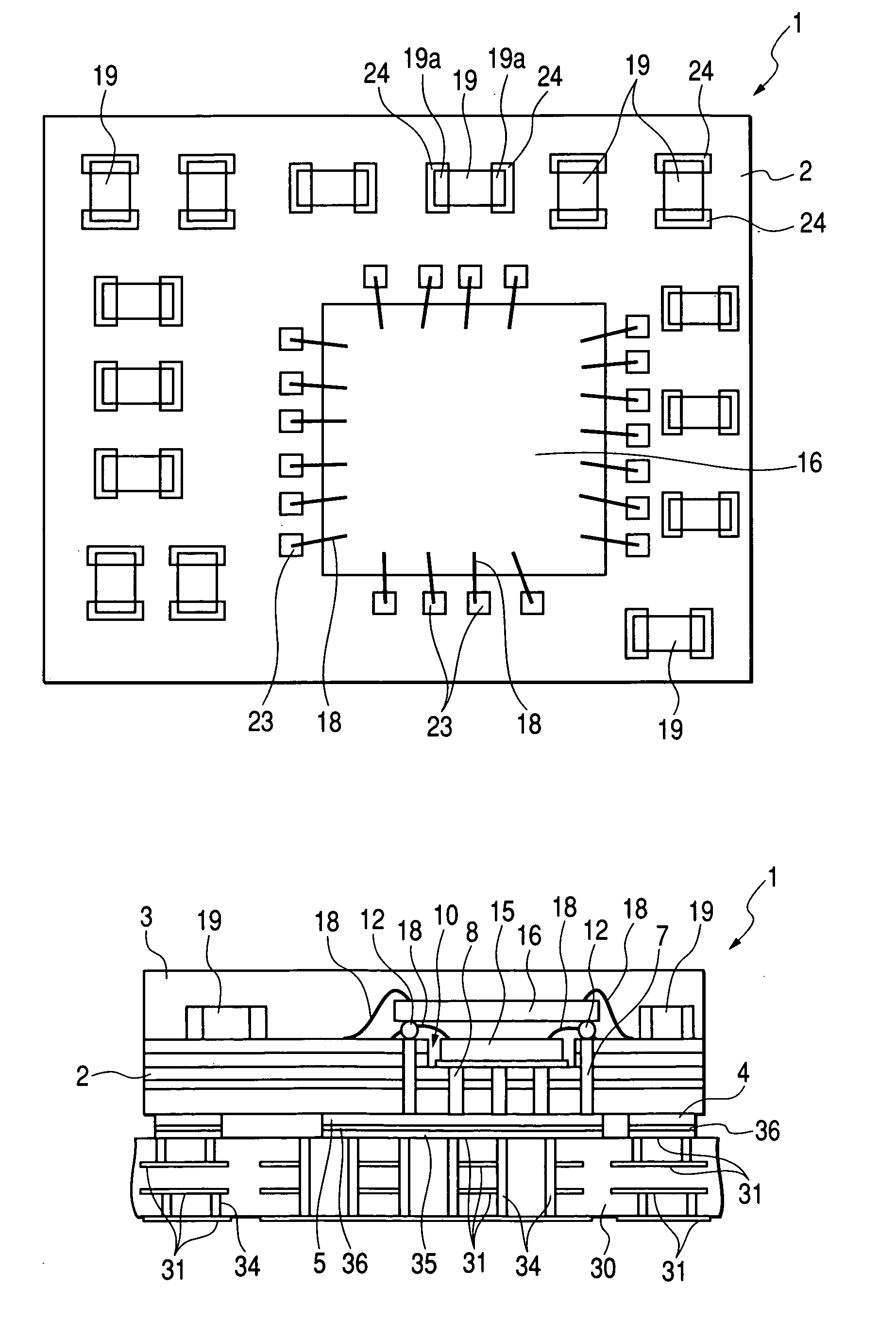
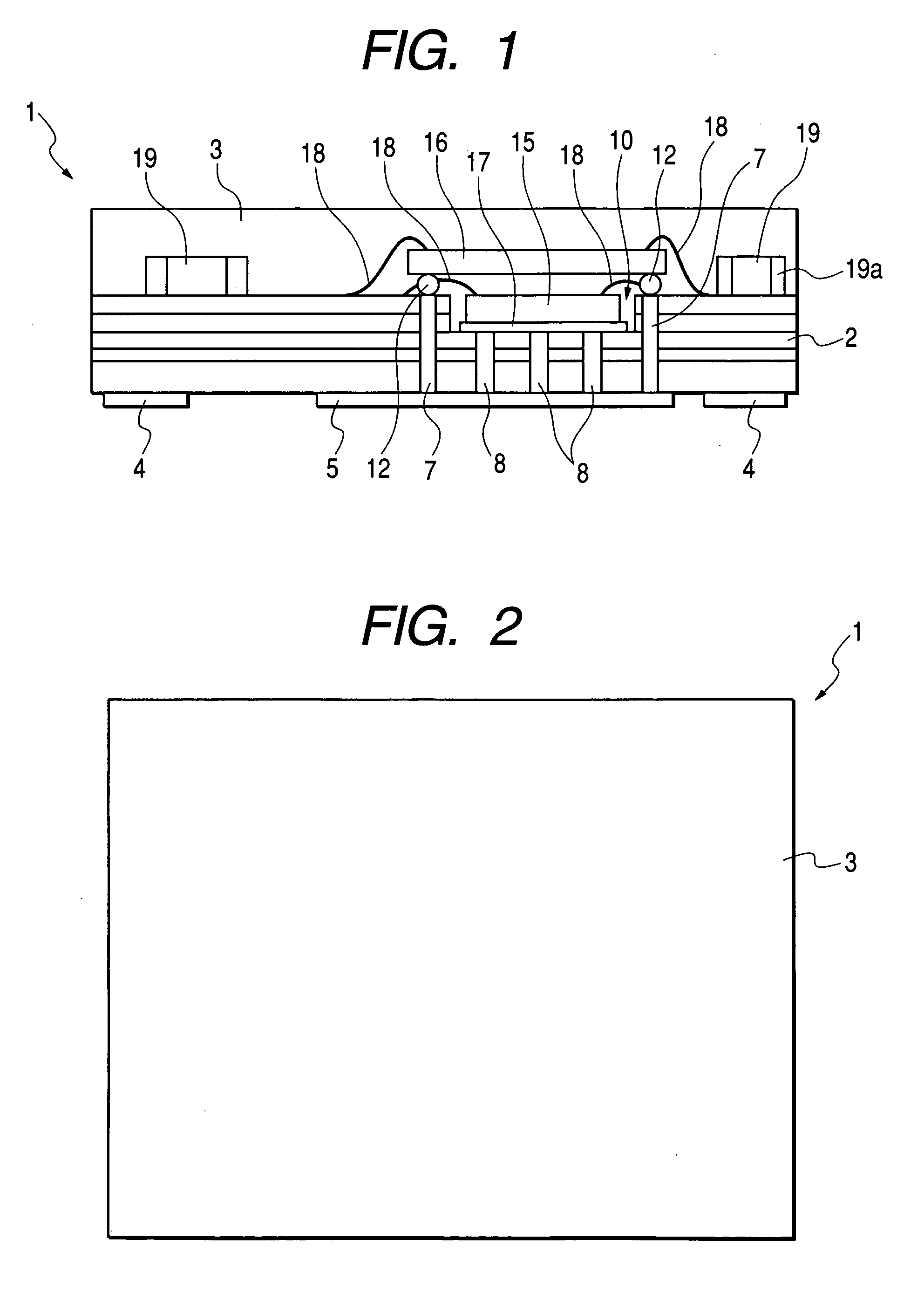
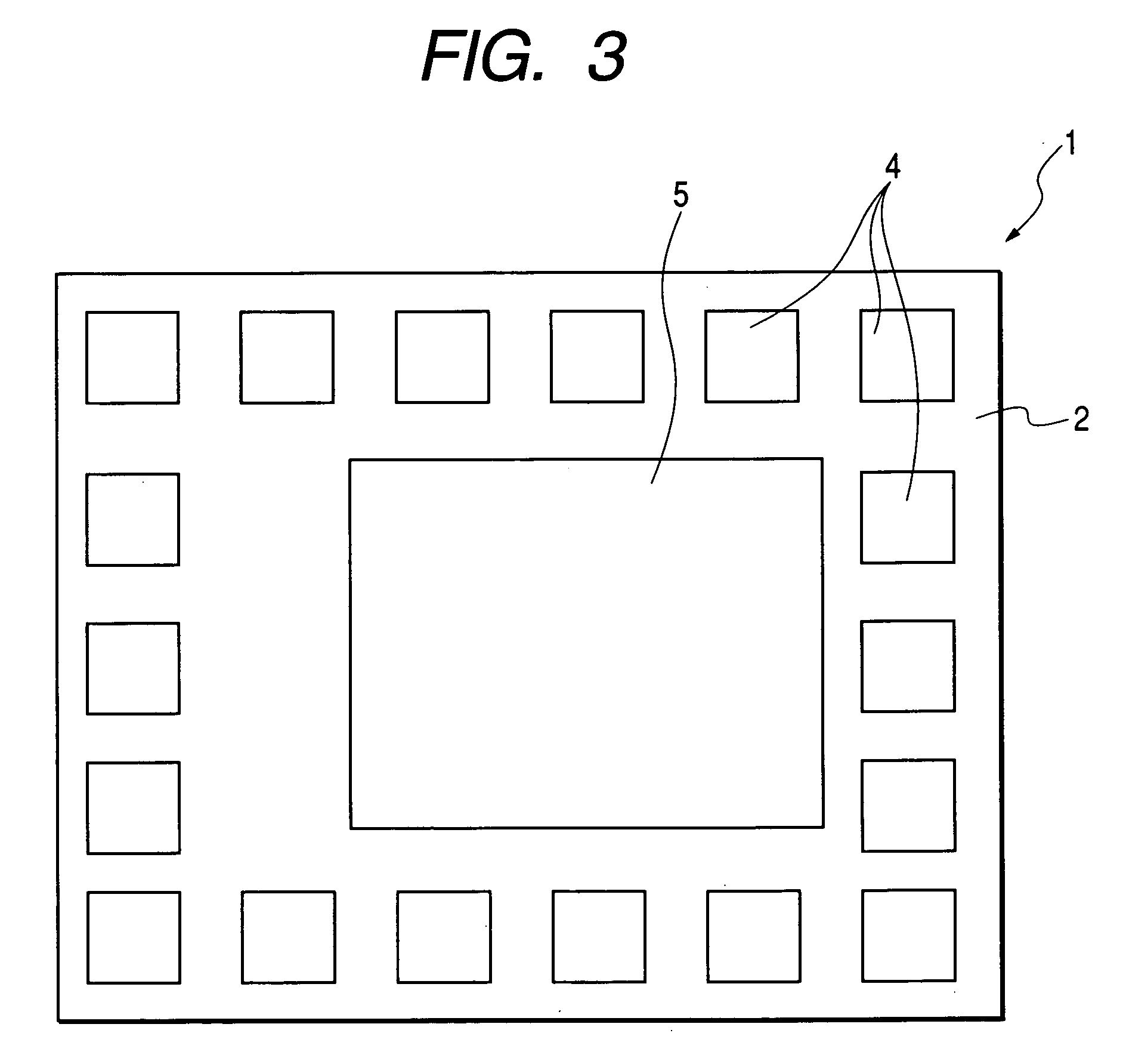
[0045]FIG. 1 to FIG. 7 are views related with a semiconductor module which constitutes one embodiment (embodiment 1) of the present invention. FIG. 1 to FIG. 5 are views related with the structure of the semiconductor module. FIG. 1 is a cross-sectional view thereof, FIG. 2 is a plan view thereof, FIG. 3 is a bottom view thereof, FIG. 4 is an enlarged cross-sectional view of a portion thereof and FIG. 5 is a schematic plan view thereof in a state that a sealing portion is removed.

[0046]The semiconductor module (semiconductor device) 1 of this embodiment 1 includes, as shown in FIG. 1 to FIG. 3, a module board 2 having a quadrangular shape in appearance, a sealing portion (a package) 3 which is formed over an upper surface of the module board 2 in an overlapped manner, and a plurality of external electrode terminals 4 and heat radiation pads 5 which are formed over a lower surface of the module board 2.

[0047]In manufacturing the semiconductor module 1, as described late...

embodiment 2

(Embodiment 2)

[0091]FIG. 9 to FIG. 11 are views related to a semiconductor module according to another embodiment (embodiment 2) of the present invention. FIG. 9 is a schematic cross-sectional view showing the semiconductor module, FIG. 10 is an enlarged cross-sectional view of a portion of the semiconductor module, and FIG. 11 is a schematic plan view of the semiconductor module in a state that a sealing portion is removed.

[0092]The semiconductor module 1 of the second embodiment 2 is characterized in that, in the semiconductor module 1 of the embodiment 1, the support bodies 12 which support the upper semiconductor chip 16 and the module board 2 are integrally formed. That is, although the support bodies 12 are formed separately from the module board 2 in the embodiment 1, the support bodies 12 are simultaneously formed at the time of manufacturing the module board 2 in the embodiment 2.

[0093]Although the dielectric layer is formed of five layers in the semiconductor module 1 of t...


PUM


Abstract

The present invention realizes strengthening of a ground of a lower-surface ground electrode of an upper semiconductor chip and miniaturization in a semiconductor module on which two semiconductor chips are mounted in a stacked manner. A lower semiconductor chip is fixed to a bottom of a recess formed in an upper surface of a module board, and an upper semiconductor chip is fixed to an upper surface of a support body made of conductor which is formed over the upper surface of the module board around the recess. External electrode terminals and a heat radiation pad are formed over a lower surface of the module board.

Description

BACKGROUND OF THE INVENTION[0001]The present invention relates to A power amplifier module, and more particularly to a power amplifier module which can arrange a plurality of semiconductor chips in a vertically stacked manner while preventing them from coming into contact with each other and, at the same time, can strengthen a ground of an upper semiconductor chip.[0002]As an example of a semiconductor module (semiconductor device) which mounts semiconductor chips in which active elements such as transistors are incorporated and chip parts in which passive elements such as resistors and capacitors are incorporated on a printed wiring board respectively, a hybrid module has been known (see Patent Reference 1, for example).[0003]Further, a product which incorporates a plurality of semiconductor chips in a package has been known (see Patent Reference 2, for example).[Patent Reference 1]Japanese Unexamined Patent Publication 2000-58741 (Pages 5 and 6, FIG. 1)[Patent Reference 2]Japanese...

Claims


Application Information

Patent Timeline
IPC IPC(8): H05K7/02H05K7/06H05K7/08H05K7/10H01L25/18H01L23/31H01L23/367H01L25/065H01L25/07H05K1/18H05K3/30
CPCH01L23/3121H01L23/3677H01L24/73H01L24/97H01L25/0657H05K3/303H01L2224/48091H01L2224/48227H01L2224/49171H01L2224/73257H01L2224/73265H01L2224/97H01L2225/0651H01L2225/06517H01L2225/06527H01L2225/06541H01L2225/06555H01L2225/06582H01L2225/06589H01L2924/01004H01L2924/01013H01L2924/01015H01L2924/01029H01L2924/0103H01L2924/01033H01L2924/01047H01L2924/01078H01L2924/01082H01L2924/13091H01L2924/15153H01L2924/1517H01L2924/19041H01L2924/19042H01L2924/19043H01L2924/19105H05K1/183H05K2201/0367H05K2201/09781H05K2201/10515H05K2201/2036H01L24/48H01L24/49H01L2924/01005H01L2924/01006H01L2924/01041H01L2224/16225H01L2224/32225H01L2924/12041H01L2224/83138H01L2224/32013H01L2924/1306H01L2224/16235H01L2924/00014H01L2924/00012H01L2924/00H01L2224/451H01L2924/181Y02P70/50H01L2224/45099H01L2224/05599H01L2224/0401
Inventor KONISHI, SATORUENDOH, TSUNEOTSUCHIYA, MASAAKINAKAJIMA, HIROKAZU
Owner RENESAS TECH CORP
Why Eureka
Try Eureka