Semiconductor memory with single cell and twin cell refreshing

a technology of memory and memory cells, applied in the field of memory of semiconductors, can solve the problems of consuming battery and reducing the number of memory cells to be refreshed, and achieve the effects of simple control, efficient change, and high speed

Inactive Publication Date: 2006-12-26
SOCIONEXT INC
View PDF11 Cites 12 Cited by
  • Summary
  • Abstract
  • Description
  • Claims
  • Application Information

AI Technical Summary

Benefits of technology

[0010]It is an object of the present invention to reduce power consumption for retaining data in a semiconductor memory having volatile memory cells.
[0011]It is another object of the present invention to realize a quick change from an operation mode for holding data to a mode for accessing data.
[0012]According to one of the aspects of the semiconductor memory of the present invention, each of a plurality of memory cell groups is constituted of a plurality of volatile memory cells connected to a predetermined number of word lines, respectively. A control circuit executes operations of a first memory mode and a second memory mode, the first memory mode being a mode in which each of the memory cells independently retains data and the second memory mode being a mode in which the memory cells in each of the memory cell groups retain the same data. The second memory mode is a mode in which a so-called partial technology and twin cell technology are combined, and in this mode, the data retained in the first memory mode is partly retained by the plural memory cells. Therefore, the data retention time of the memory cells in the second memory mode is longer than that in the first memory mode. As a result, the frequency of refreshing the memory cells can be greatly lowered, which can reduce power consumption.

Problems solved by technology

Therefore, the hand-held terminal using the DRAM as its work memory consumes power only for retaining data even when it is not in use, so that a battery is consumed.
The partial refresh technology limits memory cells that are to retain data in a standby state, thereby decreasing the number of memory cells to be refreshed.

Method used


Image

  • Semiconductor memory with single cell and twin cell refreshing
  • Semiconductor memory with single cell and twin cell refreshing
  • Semiconductor memory with single cell and twin cell refreshing

Examples


first embodiment

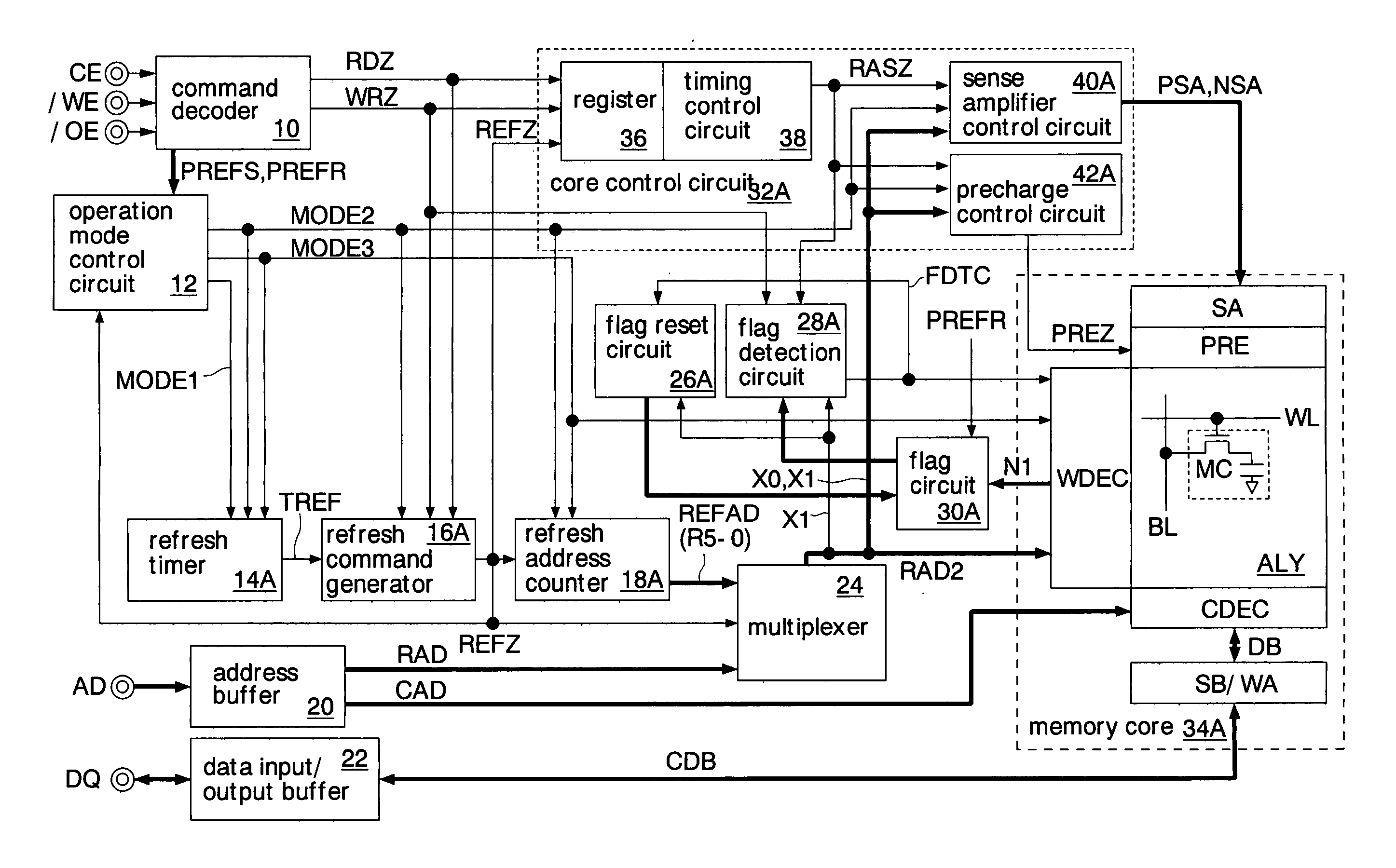
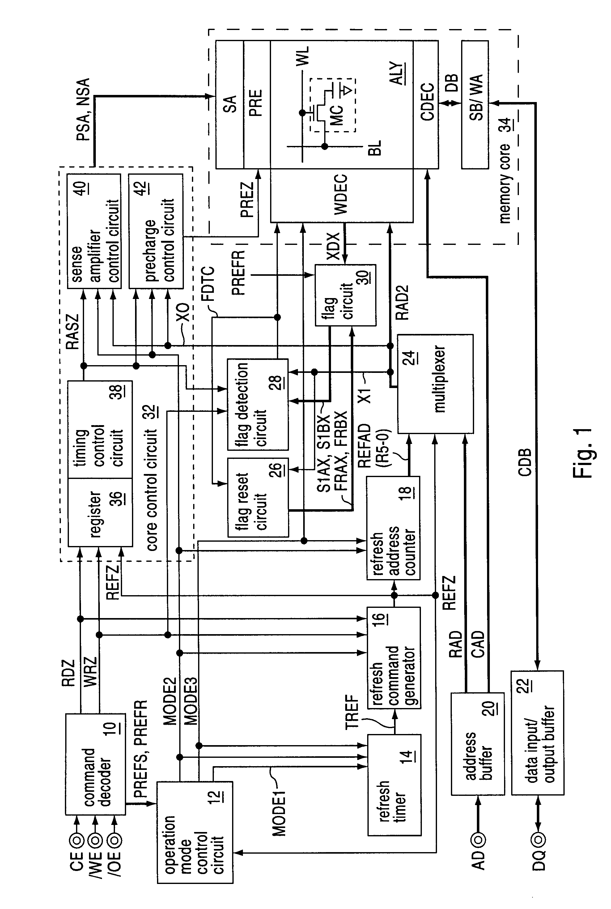
[0071]FIG. 1 shows the semiconductor memory of the present invention. This semiconductor memory is formed as a pseudo SRAM having DRAM memory cells and SRAM interfaces by using a CMOS technology. The pseudo SRAM periodically executes a refresh operation inside a chip to retain data written to memory cells without receiving any external refresh command. This pseudo SRAM is used as, for example, a work memory mounted on a cellular phone.

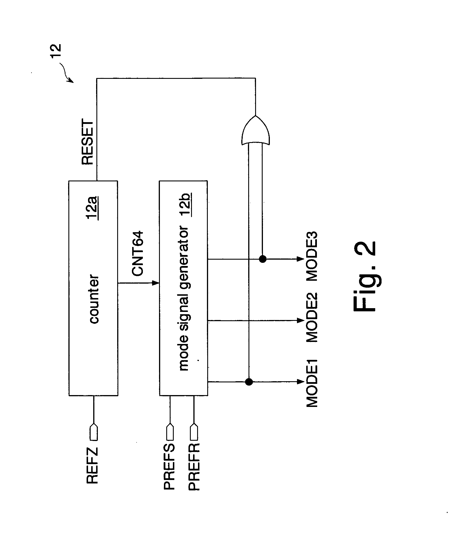
[0072]The pseudo SRAM has a command decoder 10, an operation mode control circuit 12, a refresh timer 14, a refresh command generator 16, a refresh address counter 18, an address buffer 20, a data input / output buffer 22, a multiplexer 24, a flag reset circuit 26, a flag detection circuit 28, a flag circuit 30 (flag set circuit), a core control circuit 32, and a memory core 34. The operation mode control circuit 12 and the core control circuit 32 operate as control circuits executing operations in a first and a second memory mode, which will be describe...

second embodiment

[0242]FIG. 41 shows operations during a normal operation mode in the

[0243]In the normal operation mode, similarly to the first embodiment (FIG. 20), the word lines SW0P, SW1, SW3, SW4 are independently selected according to a row address signal RAD2. Then, in response to an external read command or write command, a read operation or a write operation is executed. A refresh operation is executed in response to a refresh command internally generated in the pseudo SRAM.

[0244]FIG. 42 shows operations during a common refresh mode in the second embodiment.

[0245]In the common refresh mode, data retained in the partial memory cell C00 is first latched in the sense amplifier SA (FIG. 42(a)). Next, while the sense amplifier SA is kept activated, the common memory cells C10, C20, C30 are sequentially accessed and the data latched in the sense amplifier SA (complementary data) is written to these memory cells C10, C20, C30 (FIG. 42(b, c, d)). Consequently, the complementary data are retained in...


PUM


Abstract

Flags are formed to respectively correspond to memory cell groups each including volatile memory cells. Each flag indicates as a set state that the memory cells store data in a second memory mode. In a changing operation of changing from a first memory mode in which data is independently retained by each memory cell to a second memory mode in which same data are retained in the memory cells of each memory cell group, each flag is reset in response to the first access to the corresponding memory cell group. Therefore, only the first access is made in the second memory mode in each memory cell group. The memory cells are accessed in a mode according to the flag in the changing operation, thereby allowing a system managing the semiconductor memory to freely access the memory cells even during the changing operation. Consequently, a practical changing time can be eliminated.

Description

CROSS-REFERENCE TO RELATED APPLICATIONS[0001]This application is a continuation application of PCT International Patent Application No. PCT / JP03 / 05285, filed on Apr. 24, 2003, the entire contents of which are incorporated herein by reference.BACKGROUND OF THE INVENTION[0002]1. Field of the Invention[0003]The present invention relates to a semiconductor memory requiring a refresh operation for retaining data written to its memory cells.[0004]2. Description of the Related Art[0005]A memory capacity required for a hand-held terminal such as a cellular phone is increasing year by year. Under such circumstances, a dynamic RAM (hereinafter, referred to as a DRAM) has come into use as a work memory of the hand-held terminal in place of a conventional static RAM (hereinafter, referred to as a SRAM). Since the DRAM has a smaller number of elements constituting a memory cell than the SRAM, its chip size can be made smaller and its chip cost can be made lower than those of the SRAM.[0006]Meanw...

Claims


Application Information

Patent Timeline
Patent Type & Authority Patents(United States)
IPC IPC(8): G11C7/00G11C7/10G11C11/406G11C11/4063
CPCG11C7/1045G11C11/406G11C11/40615G11C11/40622G11C2211/4067
Inventor MATSUZAKI, YASUROU
Owner SOCIONEXT INC
Why Eureka
Try Eureka