Switchable memory diode-a new memory device

a memory diode and switchable technology, applied in the field of memory cells, can solve the problems of increasing costs, slowness of other types of storage devices, and the loss of volatile memory cells' information, and achieve the effect of significantly reducing the number of transistors required for memory cells and reducing power consumption for such arrays

Active Publication Date: 2007-01-02
MONTEREY RES LLC
View PDF10 Cites 9 Cited by
  • Summary
  • Abstract
  • Description
  • Claims
  • Application Information

AI Technical Summary

Benefits of technology

[0008]The present invention provides for systems and methods of forming diode elements integral with a memory, wherein a diode element employs an active layer (e.g. a polymer layer), and a passive layer (e.g. a super-ionic thin film), with asymmetric P / N characteristics to create a diode function. Such diode components can mitigate power consumption for memory cell arrays, and at the same time further provide for isolation of memory cells from one another, to enable an individual programming of a memory cell as part of the array.
[0009]According to one aspect of the present invention, the active and passive layer arrangement can form a component with two terminals that exhibits properties of a switchable “ON” or forward diode element with electrical isolation characteristics, which at the same time can be integral with a memory cell. The active layer can comprise: organic (e.g. conjugated polymer and related chemical compounds with N or P type properties), non-organic material, semiconducting material, and various inclusion compounds (e.g. Ti Se2). The passive and active layer can be sandwiched between ohmic contact planes. In addition, the active layer can be doped to achieve desired resistivity properties, and enable a typically precise adjustment of required threshold properties associated with the diode element. Employing the diode elements of the present invention can reduce a number of transistor-type voltage controls. Moreover, an efficient placement of polymer memory cell on a wafer surface can be obtained that increases an amount of die space available for circuit design.
[0011]In accordance with an aspect of the present invention, the diode component can enable fabrication of passive array of memory cells—wherein a number of transistors required for memory cells is greatly reduced—by enabling individual memory cells to be programmed. Accordingly, size of array employing the diode component of the present invention can be significantly condensed. Like wise, power consumption for such array can be significantly lowered.

Problems solved by technology

The long term storage mediums typically store larger amounts of information at a lower cost, but are slower than other types of storage devices.
Volatile memory cells usually lose their information if they lose power and typically require periodic refresh cycles to maintain their information.
Nonetheless, formation of various transistor type control devices that are typically required for programming memory cell arrays increase costs and reduces efficiency of circuit design.

Method used


Image

  • Switchable memory diode-a new memory device
  • Switchable memory diode-a new memory device
  • Switchable memory diode-a new memory device

Examples


Embodiment Construction

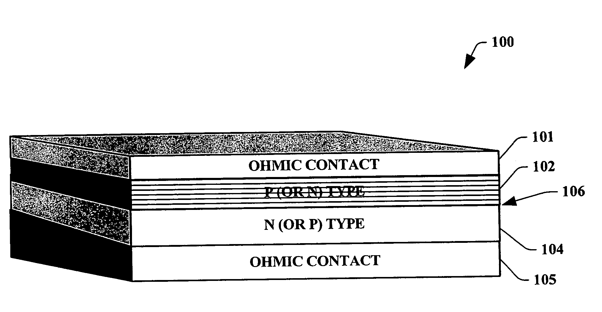
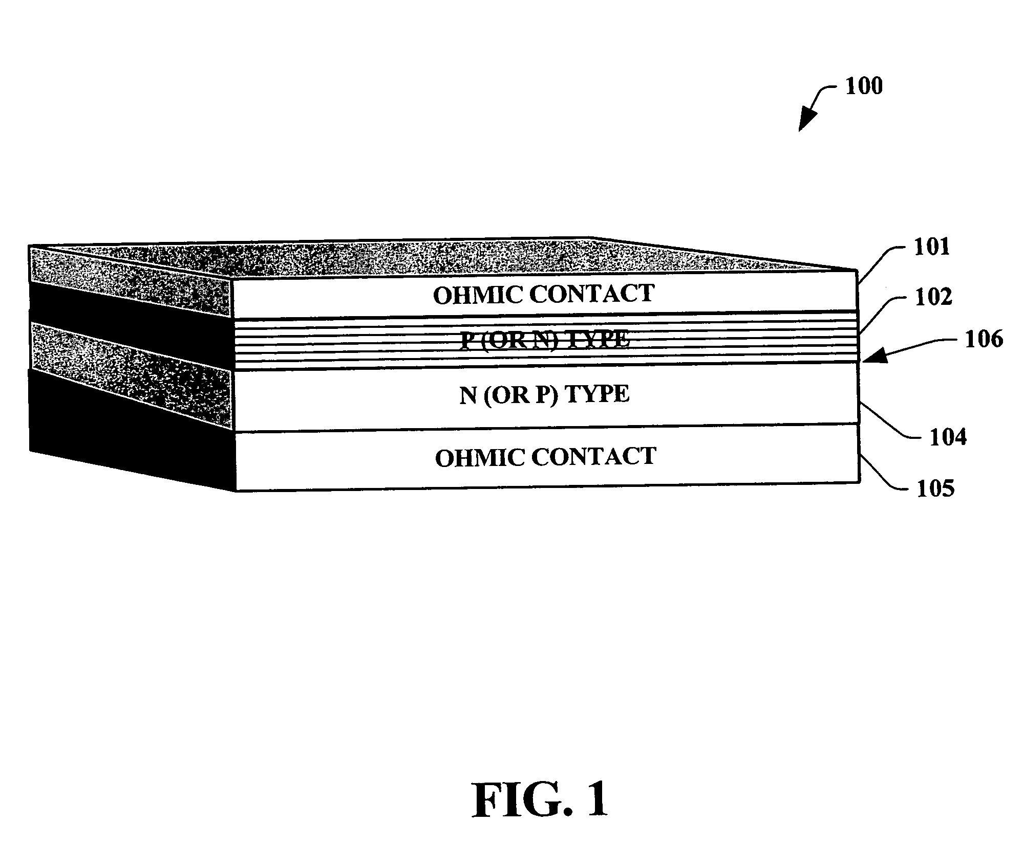
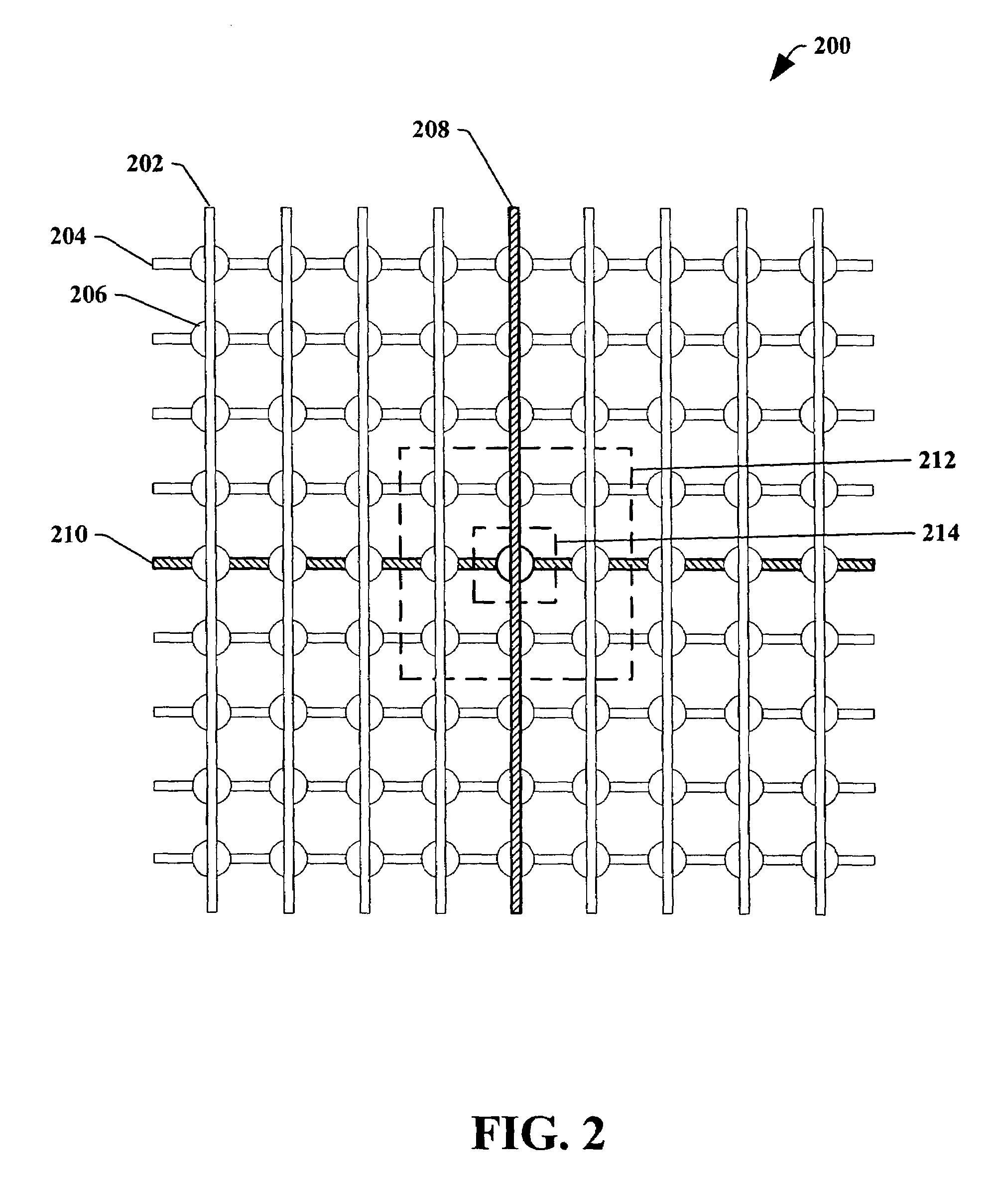
[0025]The present invention is now described with reference to the drawings, wherein like reference numerals are used to refer to like elements throughout. In the following description, for purposes of explanation, numerous specific details are set forth in order to provide a thorough understanding of the present invention. It may be evident, however, that the present invention may be practiced without these specific details. In other instances, well-known structures and devices are shown in block diagram form in order to facilitate describing the present invention.

[0026]As used herein, the term “inference” refers generally to the process of reasoning about or inferring states of the system, environment, and / or user from a set of observations as captured via events and / or data. Inference can be employed to identify a specific context or action, or can generate a probability distribution over states, for example. The inference can be probabilistic—that is, the computation of a probab...


PUM

PropertyMeasurementUnit
thicknessaaaaaaaaaa
thicknessaaaaaaaaaa
thicknessaaaaaaaaaa

Abstract

Systems and methodologies are provided for forming a diode component integral with a memory cell to facilitate programming arrays of memory cells created therefrom. Such a diode component can be part of a PN junction of memory cell having a passive and active layer with asymmetric semiconducting properties. Such an arrangement reduces a number of transistor-type voltage controls and associated power consumption, while enabling individual memory cell programming as part of a passive array. Moreover, the system provides for an efficient placement of memory cells on a wafer surface, and increases an amount of die space available for circuit design.

Description

TECHNICAL FIELD[0001]The present invention relates generally to memory cells, and in particular to a memory cell with a diode integral therewith.BACKGROUND OF THE INVENTION[0002]The proliferation and increased usage of portable computer and electronic devices has greatly increased demand for memory cells. Digital cameras, digital audio players, personal digital assistants, and the like generally seek to employ large capacity memory cells (e.g., flash memory, smart media, compact flash, or the like). Memory cells can be typically employed in various types of storage devices. Storage devices include long term storage mediums such as, for example, hard disk drives, compact disk drives and corresponding media, digital video disk (DVD) drives, and the like. The long term storage mediums typically store larger amounts of information at a lower cost, but are slower than other types of storage devices. Storage devices also include memory devices which are often, but not always, short term s...

Claims


Application Information

Patent Timeline
Patent Type & Authority Patents(United States)
IPC IPC(8): H01L29/08
CPCB82Y10/00G11C13/0009G11C13/0014G11C13/0016G11C13/003G11C13/0069H01L51/0595G11C11/5664Y10T29/41G11C2013/009G11C2213/15G11C2213/34G11C2213/56G11C2213/72G11C2213/73G11C2213/77H01L27/285H01L51/0034H01L51/0035H01L51/0036H01L51/0038H01L51/0051H01L51/0077H01L51/0078H01L51/0094H10K19/202H10K85/10H10K85/114H10K85/111H10K85/611H10K85/113H10K85/311H10K85/30H10K85/40H10K10/701G11C11/56G11C13/02H10K30/671H01L29/861
Inventor KRIEGER, JURI H.SPITZER, STUART
Owner MONTEREY RES LLC
Why Eureka
Try Eureka