Light emitting diode and manufacturing method thereof

a technology of light-emitting diodes and manufacturing methods, which is applied in the direction of semiconductor devices for light sources, light-emitting devices, fixed installations, etc., can solve the problems of reduced device life, reduced luminous efficiency, and heat dissipation, and achieve enhanced heat-emitting efficiency from the light-emitting portion

Inactive Publication Date: 2007-01-09
TOYODA GOSEI CO LTD
View PDF16 Cites 35 Cited by
  • Summary
  • Abstract
  • Description
  • Claims
  • Application Information

AI Technical Summary

Benefits of technology

[0013]Another object of the present invention is to provide a light shielding / reflecting type device, which shows high efficiency in external radiation of light and high contrast between the intensity of light, which is radiated during the light source is turned on, and that of light reflected when the light source is turned off, and to provide a light source therefor.
[0062]Thus, the light source portion is mounted on the heat radiation conductive member of the substrate portion. The heat radiation conductive member leads to the back surface of the substrate portion. Consequently, heat outputted from the light source portion is transmitted to the rear side of the substrate portion through the heat radiation conductive member. Thus, the efficiency in radiation of heat outputted from the light source portion is enhanced very much. To sum up, according to the present invention, there is provided a light emitting diode comprising: a substrate having a heat radiation conductive member therein; and a light emitting element mounted on said substrate, at least a part of said light emitting element being directly brought into contact and electrically connected with said heat radiation conductive member.

Problems solved by technology

Thus, this conventional light emitting diode has drawbacks in that heat dissipation is poor, that consequently, the temperature of the light emitting element 52 rises to a high level, and luminous efficiency lowers, and device lifetime decreases.
However, the conventional reflective LED 131 has problems in that because the area of the reflecting surface seen from the outside is large, large dark noises are caused (that is, what is called pseudo-lighting occurs) owing to the reflection of external light at each turn-off of the light source, and that consequently, the contrast between the intensity of the light, which is radiated during the light source is turned on, and that of the light reflected when the light source is turned off, is low.

Method used


Image

  • Light emitting diode and manufacturing method thereof
  • Light emitting diode and manufacturing method thereof
  • Light emitting diode and manufacturing method thereof

Examples


first embodiment

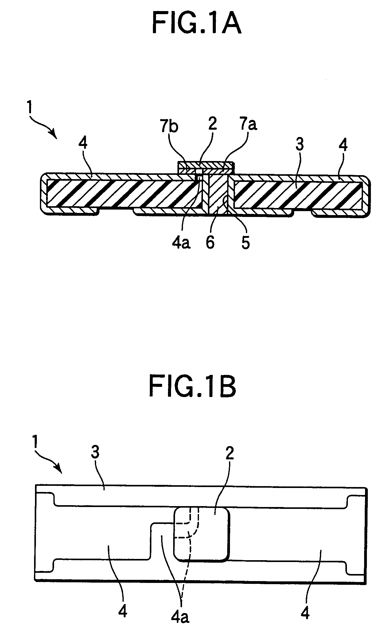
[0078]First, a first embodiment of the invention is described with reference to FIGS. 1A and 1B. FIG. 1A is a longitudinally sectional view illustrating the entire configuration of a light emitting diode according to the first embodiment of the invention. FIG. 1B is a plan view thereof.

[0079]As illustrated in FIG. 1A, in an LED 1 of the first embodiment, a through hole 5 is drilled in a glass epoxy resin substrate. Moreover, a GaN light emitting element 2 is mounted on a through-hole substrate 3 having a conductive pattern 4 printed on the top and bottom surfaces thereof and on the inner surface of the through hole 5. The through hole 5 is filled with solder 6 acting as metal (heat radiation conductive member). One of the rear surface electrodes of the light emitting element 2 is electrically connected onto this through hole 5 by a gold bump 7a, while the other rear surface electrode is electrically connected to the side, which is insulated from the through hole 5, of the conductive...

second embodiment

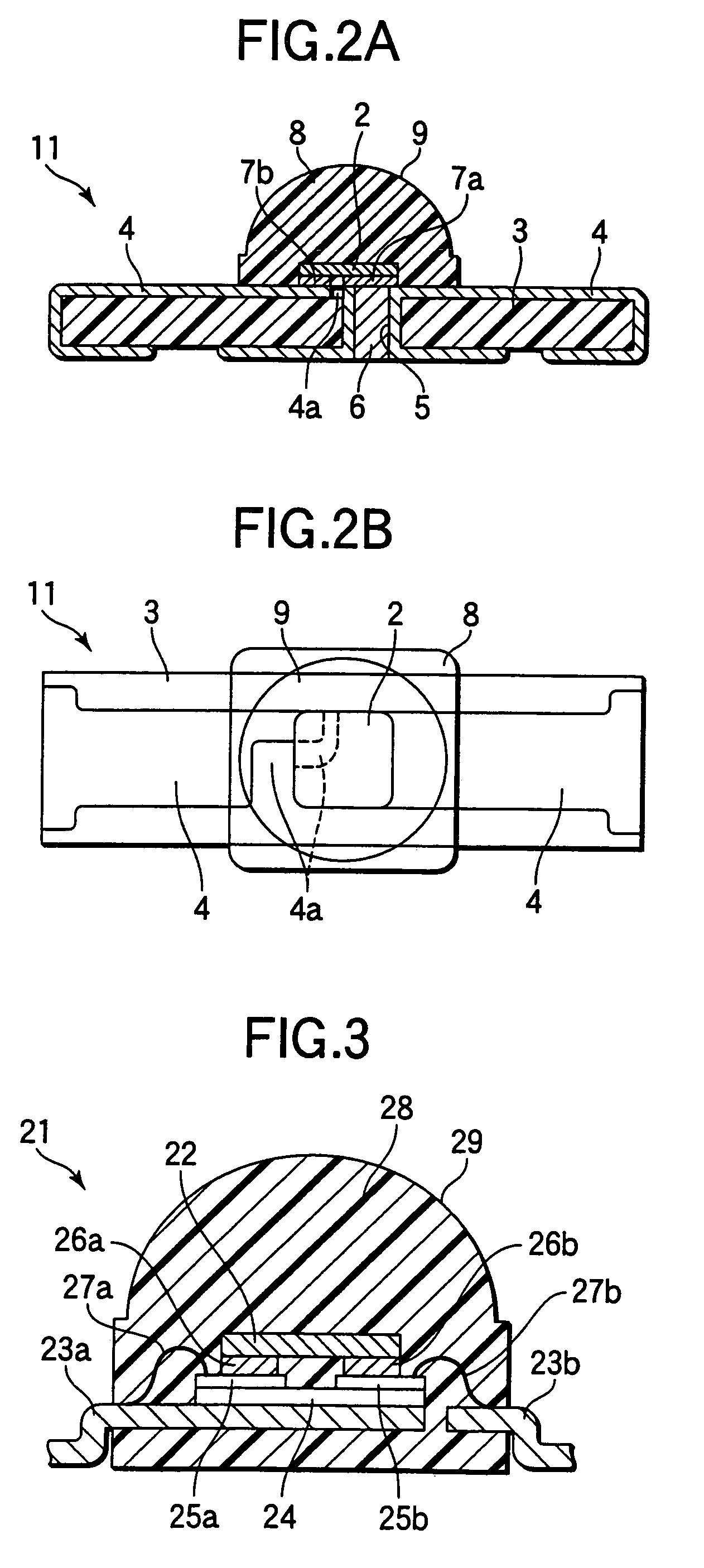
[0084]Next, a second embodiment of the invention is described hereinafter with reference to FIGS. 2A and 2B. FIG. 2A is a longitudinally sectional view illustrating the entire configuration of a light emitting diode according to the second embodiment of the invention. FIG. 2B is a plan view thereof. Incidentally, like reference numerals designate like components of the first embodiment. Further, the description of such components is omitted herein.

[0085]As illustrated in FIGS. 2A and 2B, the LED 11 of this second embodiment differs from the LED 1 of the first embodiment in that in the former LED, the light emitting element 2 and a part of the through hole substrate 3 are sealed with transparent epoxy resin 8 serving as the light transmissive material, and that a light-emitting-surface-side part thereof is a convex lens 9 serving as a light radiating surface portion.

[0086]Thus, the quantity of light radiated from the light emitting element is increased by sealing the light emitting e...

third embodiment

[0088]Next, a third embodiment of the invention is described hereinbelow with reference to FIG. 3. FIG. 3 is a longitudinally sectional view illustrating the entire configuration of a light emitting diode according to the third embodiment of the invention.

[0089]As illustrated in FIG. 3, in an LED 21 of this third embodiment, an insulating film 24, on which copper foils 25a and 25b serving as two conductive foils are provided apart from each other, is stuck onto one 23a of a pair of leads 23a and 23b for supplying electric power to a GaN light emitting element 22. The thickness of the insulating film 24 is about 100 μm, while the thickness of the copper foils 25a and 25b is about 20 μm. Thus, the two rear surface electrodes are connected to the insulated two copper foils 25a and 25b by gold bumps 26a and 26b, respectively. Further, the surface of the copper foil 25a is electrically connected to one 23a of the leads by bonding using a wire 27a. Furthermore, the surface of the copper f...


PUM


Abstract

A light emitting diode has a substrate having a heat radiation conductive member therein, and a light emitting element mounted on the substrate. At least a part of the light emitting element is directly brought into contact and electrically connected with the heat radiation conductive member.

Description

[0001]The present Application is a Divisional Application of U.S. patent application Ser. No. 10 / 102,813 filed on Mar. 22, 2002 now U.S. Pat. No. 6,833,566.[0002]The present application is based on Japanese Patent Applications Nos. 2001-091961 and 2001-308256, which are incorporated herein by reference.BACKGROUND OF THE INVENTION[0003]1. Field of the Invention[0004]The present invention relates to what is called a flip-chip-type light emitting diode (hereunder sometimes abbreviated as “an LED”) adapted so that a light emitting element is electrically connected to leads through the rear surface electrode thereof. The present invention also relates to a light shielding / reflecting type device adapted so that light outputted from a light source is reflected by a concave reflecting mirror and that the reflected light is radiated from an optical opening portion provided in a light shielding plate, and to the light source therefore. Incidentally, in the present specification, an LED chip i...

Claims


Application Information

Patent Timeline
Patent Type & Authority Patents(United States)
IPC IPC(8): H01L29/22H01L29/227H01L33/00F21S8/10F21V11/12F21V13/10H01L33/54H01L33/60H01L33/64
CPCF21V29/74F21V29/004H01L33/60H01L33/647F21S48/328F21S48/215F21V11/12F21V13/10F21Y2101/02H01L33/54H01L2924/3025H01L2224/48247H01L2224/48091H01L2224/13H01L2924/00H01L2924/00014F21Y2115/10F21S43/14F21V29/83H01L2224/0401
Inventor SUEHIRO, YOSHINOBUKATO, HIDEAKIHADAME, KUNIHIRO
Owner TOYODA GOSEI CO LTD
Why Eureka
Try Eureka