

Semiconductor memory device with on die termination circuit
a semiconductor memory device and termination circuit technology, applied in the direction of digital transmission, pulse technique, instruments, etc., can solve the problems of increasing power consumption, data transferring operation not being stably operated, semiconductor memory devices cannot stably receive data, etc., and achieve the effect of reducing power consumption for performing an on die termination operation
- Summary
- Abstract
- Description
- Claims
- Application Information
AI Technical Summary
Benefits of technology
Problems solved by technology
Method used
Image

Examples
first embodiment
[0044]FIG. 5 is a schematic circuit diagram showing an on die termination circuit for use in a semiconductor memory device in accordance with the present invention.
[0045]As shown, the on die termination circuit includes a data input / output pad (DQ pad) for inputting / outputting data; a data input buffer 60 for buffering an output data outputted from the DQ pad; an on die termination pad DQ_ODT for receiving an on die termination voltage VTT from an external circuit; an on die termination resistor RTT3 connected between the on die termination pad DQ_ODT and the DQ pad; and a switch SW3 for connecting the on die termination resistor RTT3 to the on die termination pad DQ_ODT. The DQ pad is connected to the data input buffer 60 and a data output buffer 70.
[0046]Herein, the switch SW3 can be formed by a metal oxide semiconductor (MOS) transistor. The termination resistor RTT3 is a variable resistor capable of changing a resistance. When the switch SW3 is turned on, the on die termination ...
second embodiment
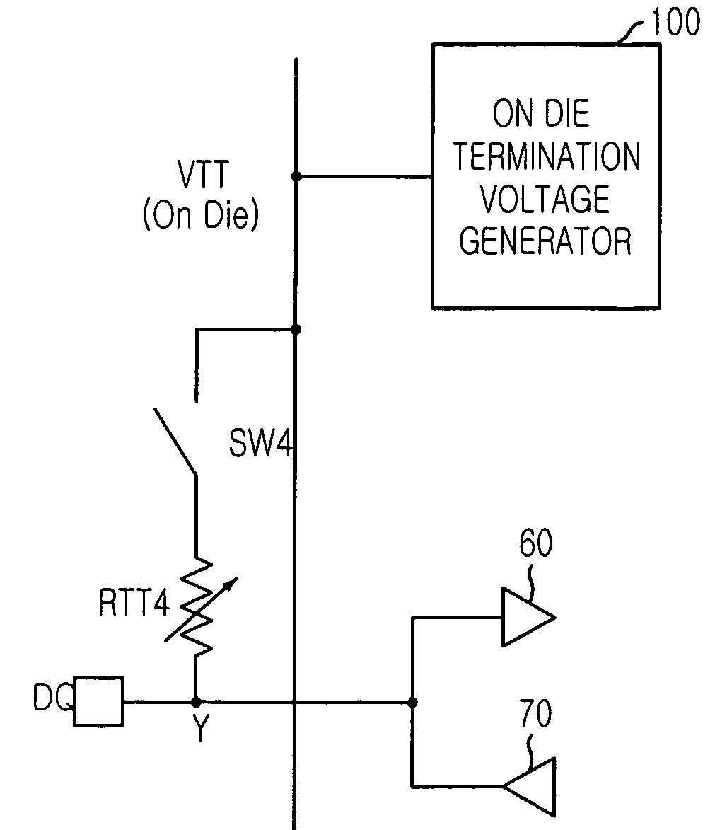
[0050]FIG. 6 is a schematic circuit diagram showing an on die termination circuit in accordance with the present invention.
[0051]As shown, the on die termination circuit includes a data input / output pad (DQ pad) for inputting / outputting data; a data input buffer 60 for buffering an output data outputted from the DQ pad; an on die termination voltage generator 100 for generating an on die termination voltage VTT; an on die termination resistor RTT4 one end of which is connected to the DQ pad; and a switch SW4 for connecting the on die termination voltage VTT to the on die termination resistor RTT4 while data are inputted to the data input buffer 60. The DQ pad is connected to the data input buffer 60 and a data output buffer 70.
[0052]Herein, a voltage level of the termination voltage VTT is adjusted so that a voltage level of at an input node Y can be half of a voltage level of a power supply voltage VDD. The on die termination resistor RTT4 is a variable resistor capable of changing...
third embodiment
[0056]FIG. 7 is a schematic circuit diagram depicting an on die termination circuit in accordance with the present invention.
[0057]As shown, the on die termination circuit includes a data input / output pad (DQ pad); a data input buffer 60 for buffering an output data outputted from the DQ pad; an on die termination pad DQ_ODT for receiving a first on die termination voltage VTT1 from an external circuit; an on die termination voltage generator 100 for generating a second on die termination voltage VTT; an on die termination resistor RTT5 one end of which is connected to the DQ pad; and a switch SW5 for connecting the first on die termination voltage VTT1 or the second on die termination voltage VTT2 to the on die termination resistor RTT5 while data are inputted to the data input buffer 60. The DQ pad is connected to the data input buffer 60 and a data output buffer 70.
[0058]Herein, the termination resistor RTT5 is a variable resistor capable of changing a resistance.
[0059]Meanwhile,...
PUM
 Abstract
Description
Claims
Application Information