Method of forming nanofluidic channels

a nanofluidic channel and nanofluidic technology, applied in the direction of fluid speed measurement, material analysis, individual molecule manipulation, etc., can solve the problems of limited process to commercial applications, partial or complete filling of channels, and many technological challenges, so as to facilitate low-cost and high-volume manufacturing of nanofluidic channels

Inactive Publication Date: 2007-01-30
RGT UNIV OF MICHIGAN
View PDF13 Cites 21 Cited by
  • Summary
  • Abstract
  • Description
  • Claims
  • Application Information

AI Technical Summary

Benefits of technology

[0007]It is therefore the object of this invention to provide a simple method of fabricating nanofluidic channels with dimensions down to tens of nanometers, which facilitates low-cost and high-volume manufacturing of nanofluidic channels for a wide range of applications.

Problems solved by technology

Despite the relative ease of constructing nanoscale structures, the sealing of these nanoscale structures into functional nanofluidic channel devices often leads to many technological challenges.
The high temperature and high voltage typically used in the anodic bonding process greatly limit the process to commercial applications; while the bonding of soft elastomeric material, such as PDMS, to nanofluidic channels being about 100 nm or less in size often results in the partial or complete filling of the channel due to the rubber-like behavior of the soft elastomeric material.
However, the removal of this sacrificial layer in nano-channels is non-trivial.
In fact, via holes are often necessary to reduce the time needed to remove the sacrificial layer to a reasonable duration, which consequently increases the device complexity and fabrication cost.
Still this involves deposition machines and is a time-consuming and complex process that requires careful control of the non-uniformity during the deposition process.

Method used


Image

  • Method of forming nanofluidic channels
  • Method of forming nanofluidic channels
  • Method of forming nanofluidic channels

Examples


Embodiment Construction

[0019]The following description of the preferred embodiment(s) is merely exemplary in nature and is in no way intended to limit the invention, its application, or uses.

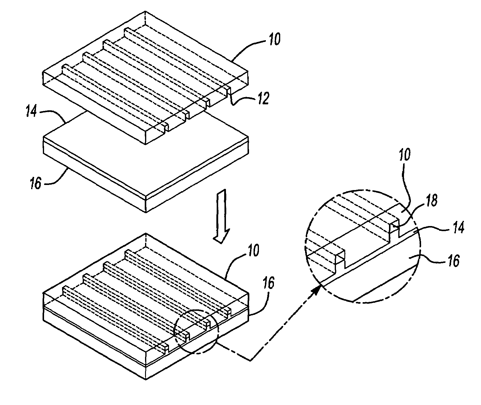
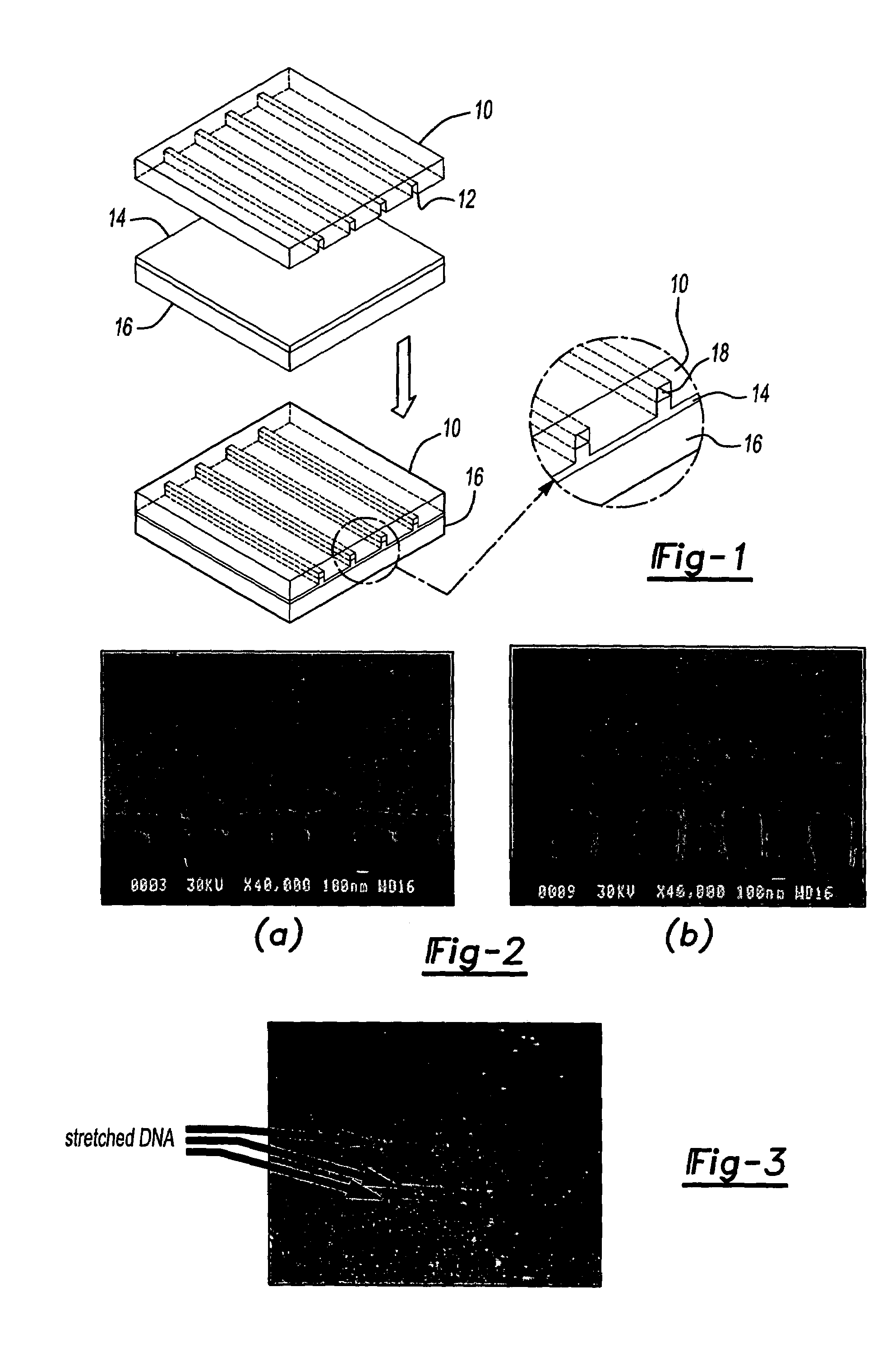
[0020]According to the teachings of the present invention, a method is provided that includes directly forming fluidic channels by a 2-step nanoimprinting technique. With particular reference to FIG. 1, which illustrates a schematic of the preferred method, a nano-channel template 10 with nanoscale trenches 12 is fabricated by a first nanoimprinting and reactive ion etching (RIE) process in oxide. Then nano-channel template 10 is used as a mold (preferably without surfactant coating) to imprint into a thin polymer layer 14 on a substrate 16 through a second nanoimprinting process. A thickness of polymer layer 14 is carefully chosen such that polymer layer 14 will not completely fill nanoscale trenches 12 of nano-channel template 10. The portions of nanoscale trenches 12 of nano-channel template 10 that remain unfilled...


PUM

PropertyMeasurementUnit
persistence lengthaaaaaaaaaa
sizeaaaaaaaaaa
widthaaaaaaaaaa

Abstract

A method of forming nanofluidic enclosed channels includes providing a first substrate having a layer of a first material disposed thereon. A plurality of nanoscale slots is formed along a second substrate using nanolithography, etching, or other disclosed techniques. The first substrate is then bonded to the second substrate such that the layer of the first material on the first substrate is adjacent the plurality of slots on the second substrate to define a plurality of enclosed nanofluidic channels therethrough.

Description

CROSS-REFERENCE TO RELATED APPLICATIONS[0001]This application claims the benefit of U.S. Provisional Application No. 60 / 379,878, filed on May 13, 2002. The disclosure of which is incorporated herein by reference.FIELD OF THE INVENTION[0002]The present invention generally relates to the construction of fluidic channels and, more particularly, relates to a simple and convenient method of constructing nanofluidic channels of various types. The method of the present invention is particularly useful in the manipulation and detection of bimolecular (especially DNA molecules) using nanostructured fluidic channels.BACKGROUND OF THE INVENTION[0003]Nano-scale fluidics (hereinafter “nanofluidic”) is an emerging field of study that has significant technological advantages. For example, the interaction of biomolecules (such as DNA) with nanostructured channels having dimensions close to the persistence length of a molecule (˜50 nm) permits an entirely new way of detecting and separating molecule...

Claims


Application Information

Patent Timeline
Patent Type & Authority Patents(United States)
IPC IPC(8): B32B3/00B32B37/02B32B1/00B82B3/00B01L3/00B81B1/00B82B1/00G01N21/05
CPCB01L3/502707B81C1/00119B82Y30/00B01L3/502715Y10S977/78B01L2200/12B01L2300/0681B01L2300/0896B01L2400/0418B01L2400/0421B01L2400/086B81B2201/058B81B2203/0338B81C2201/0153G01N2021/058Y10S977/84Y10S977/882
Inventor GUO, LINGJIE JCHENG, XING
Owner RGT UNIV OF MICHIGAN
Why Eureka
Try Eureka