Process for laser processing and apparatus for use in the same

Inactive Publication Date: 2007-01-30
SEMICON ENERGY LAB CO LTD
View PDF88 Cites 10 Cited by
  • Summary
  • Abstract
  • Description
  • Claims
  • Application Information

AI Technical Summary

Benefits of technology

[0017]Another embodiment according to the process of the present invention provides a technology for doping of an impurity from a gas phase using a laser, particularly an excimer laser, in which a plurality of elements are doped using different types of doping gases. An object of the present process using a single laser beam is to avoid the drop in doping efficiency due to the use of various doping gases differing in light absorption properties and in decomposition behavior. Accordingly, in the present process comprising irradiating a laser beam to the sample in a reactive gas atmospher

Problems solved by technology

It is unfavorable to heat the semiconductor to an excessively high tempe

Method used


Image

  • Process for laser processing and apparatus for use in the same
  • Process for laser processing and apparatus for use in the same
  • Process for laser processing and apparatus for use in the same

Examples


example 1

[0056]An N-channel thin film gate-insulated field-effect transistor (referred to hereinafter as “NTFT”) established on a glass substrate was fabricated according to a doping process of the present invention. A glass substrate or a quartz substrate was used in this example. Such substrates were selected because the TFTs thus fabricated were intended for switching devices and driving devices of an active matrix liquid crystal display device or an image sensor. The process according to the present invention can be used as a doping technology in the fabrication of other semiconductor devices as well, such as the fabrication of P-type and N-type semiconductor layers of a photoelectric conversion devices, and the fabrication of single crystal semiconductor integrated circuits (ICs). In such cases, single crystal and polycrystalline substrates of silicon and other semiconductors can be used as well as other insulators.

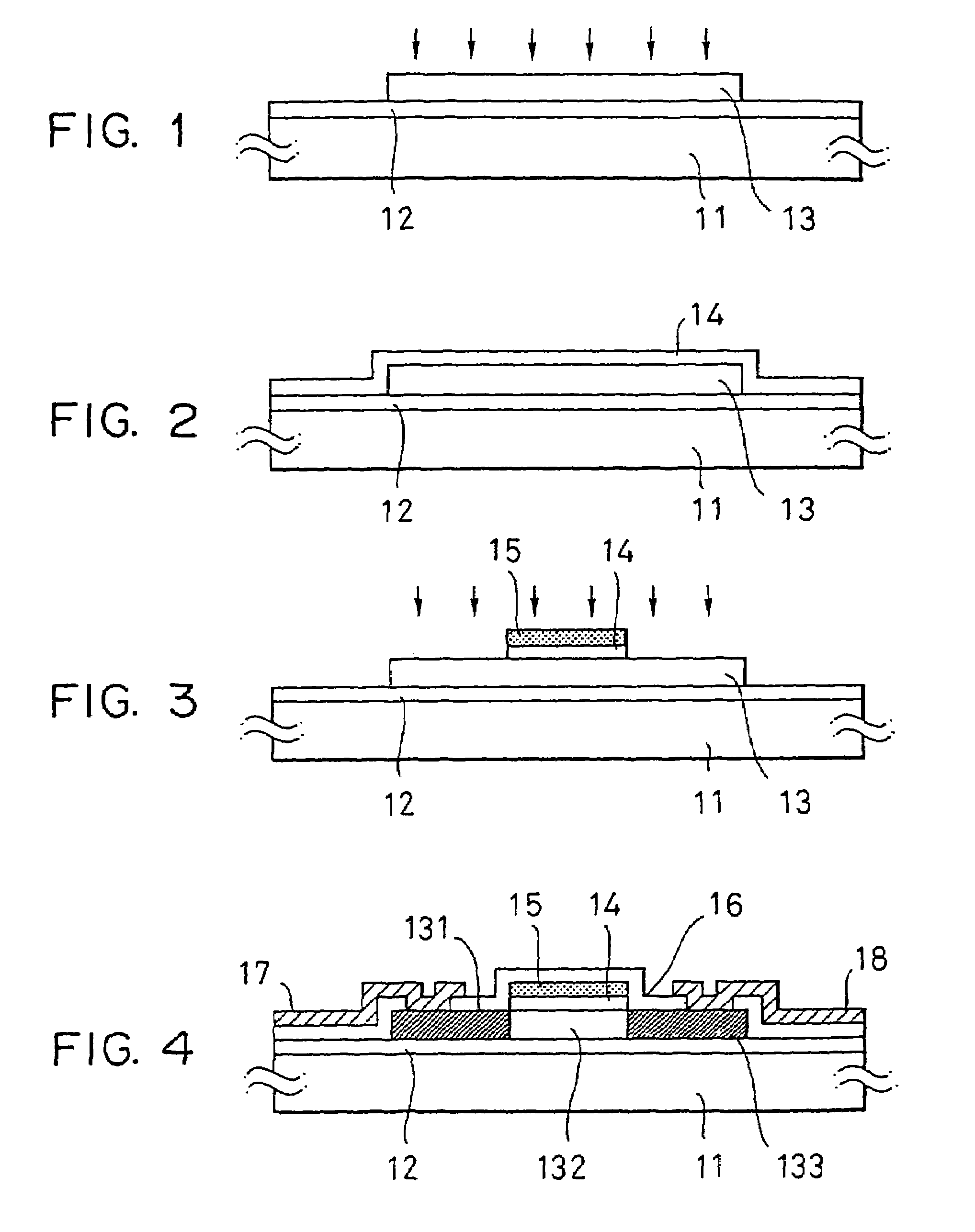
[0057]Referring to FIG. 1, the fabrication process is described. An SiO2...

example 2

[0088]An NTFT established on a glass substrate was fabricated according to a doping process of the present invention. A glass substrate or a quartz substrate was used in this example as in Example 1. Then, an SiO2 film or a silicon nitride film was first deposited on a glass substrate 11 to give a base protective film 12 as shown in FIG. 1, following the same process described in Example 1.

[0089]Then, a 100 nm thick layer 13 of hydrogenated amorphous silicon semiconductor, which is intrinsic semiconductor or substantially intrinsic, was deposited on the SiO2 film by plasma-assisted CVD process. A patterning process was then carried out to separate the film into devices to obtain a structure as shown in FIG. 1. Subsequent to the patterning, the sample was heated in vacuum (of 10−6 Torr or lower) at 450° C. for an hour to thoroughly drive out hydrogen therefrom to form dangling bonds in high density.

[0090]In the same chamber in which the process of driving out hydrogen was performed, ...

example 3

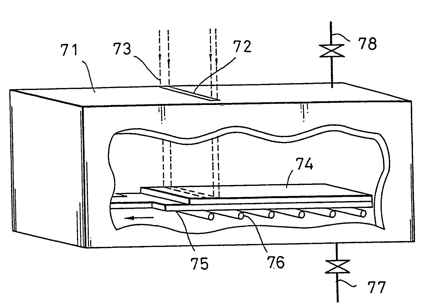
[0104]In FIG. 7 is shown a doping apparatus according to the present invention, which comprises a chamber 71 provided with an anhydrous quartz slit window 72 through which a laser beam shaped into a thin rectangular form is irradiated to the sample. This laser beam is shaped, for example, into a rectangle 10 mm by 300 mm in size. The position of the laser beam is fixed. To the chamber are further connected an evacuation system 77 and an inlet system 78 for supplying the reactive gas. In the inside of the chamber are provided a sample holder 75 on which a sample 74 is mounted, and an infrared-emitting lamp 76 as a heater is set under the sample holder. The sample holder is movable so that the sample may be moved in accordance with the laser shots.

[0105]An apparatus equipped with a mechanism for moving the sample therein requires much care in its temperature control, because the mechanism may suffer mal-alignment due to dimensional change thereof caused by the heat generated by the he...


PUM

PropertyMeasurementUnit
Temperatureaaaaaaaaaa
Melting pointaaaaaaaaaa
Semiconductor propertiesaaaaaaaaaa

Abstract

A process for laser processing an article which comprises: heating the intended article to be doped with an impurity to a temperature not higher than the melting point thereof, said article being made from a material selected from a semiconductor, a metal, an insulator, and a combination thereof; and irradiating a laser beam to the article in a reactive gas atmosphere containing said impurity, thereby allowing the impurity to physically or chemically diffuse into, combine with, or intrude into said article. The present invention also provides an apparatus for use in a laser processing process, characterized by that it is provided with an internal sample holder and a device which functions as a heating means of the sample, a window made of a material sufficiently transparent to transmit a laser beam, a chamber comprising a vacuum evacuation device and a device for introducing a reactive gas containing an impurity element, a laser apparatus operating in a pulsed mode to irradiate a laser beam to said chamber, and a means to move said chamber synchronously with the laser irradiation.

Description

[0001]This application is a DIV of Ser. No. 09 / 356,376, filed Jul. 19, 1999, now U.S. Pat. No. 6,655,767, which is a DIV of Ser. No. 09 / 145,543, filed Sep. 2, 1998, now U.S. Pat. No. 6,358,784, which is a DIV of Ser. No. 08 / 411,973, filed Mar. 28, 1995, now U.S. Pat. No. 5,849,043, which is a DIV of Ser. No. 07 / 971,237, filed Nov. 4, 1992, now U.S. Pat. No. 5,424,244.BACKGROUND OF THE INVENTION[0002]1. Field of the Invention[0003]The present invention relates -to a technique which allows conducting a doping process or other chemical and physical treatments efficiently even at a low temperature.[0004]2. Prior Art[0005]Known processes for doping semiconductors with impurities include a diffusion process and an ion implantation process. The diffusion process comprises heating the semiconductor to a high temperature in the range of from 1000 to 1200° C. to make the impurities diffuse into semiconductors. In an ion implantation process, a predetermined portion of a semiconductor is bomba...

Claims


Application Information

Patent Timeline
IPC IPC(8): H01L21/50H01L21/44H01L21/48B60R25/00E05B67/06E05B67/38H01L21/223H01L21/336
CPCB60R25/066E05B67/063E05B67/38H01L21/223H01L27/14692H01L29/66757Y10T29/41E05B2067/386
Inventor ZHANG, HONGYONGYAMAZAKI, SHUNPEITAKEMURA, YASUHIKO
Owner SEMICON ENERGY LAB CO LTD
Why Eureka
Try Eureka