
Plating method and plating apparatus

a plating apparatus and plating method technology, applied in the direction of electrolysis process, semiconductor devices, electrolysis components, etc., can solve the problems of complex operational details, loss of in-plane uniformity of plated films, and difficulty in satisfying these requirements, and achieve excellent in-plane uniformity and excellent embeddability

Active Publication Date: 2007-01-30
EBARA CORP
View PDF3 Cites 43 Cited by
  • Summary
  • Abstract
  • Description
  • Claims
  • Application Information

AI Technical Summary

Benefits of technology

"The present invention provides a plating method and apparatus that can deposit a plated film with excellent in-plane uniformity and embeddability. The plating method involves using a plating solution with a high acid concentration and an anode solution with a low acid concentration. The electric conductivity of the plating solution is reduced to increase in-plane uniformity of the plated film, while the electric conductivity of the anode solution is increased to increase embeddability of the plated film. The acid concentration in the plating solution is preferably at least 0.4 mole / L, and the anode solution should have an acid concentration of at most 0.6 mole / L. The electric conductivity of the anode solution should be managed to keep it constant at most 200 mS / cm. The plating solution and the anode solution should be separated from each other by an ion exchanger. The plating apparatus includes a substrate stage, a cathode portion, an electrode head, a plating solution inlet section, an anode solution introducing section, and a power source. A partition with an ion exchanger can be used to separate the plating solution and the anode solution."

Problems solved by technology

Difficulty will be experienced in satisfying these requirements because barrier and seed layers are expected to be much thinner in the 65 nm generation technology.
Therefore, in-plane uniformity of the plated film is lost.
However, since components used or a process recipe is changed depending on a type of plating solution and thickness of the seed layer, this solution would require complex operational details if a wide variety of samples are to be fabricated.
In particular, the above problem manifests itself for interconnects having a width of at most 0.1 μm and via holes having a diameter of at most 0.1 μm, thereby failing to embed a plated film reliably in those interconnects and via holes.
Other conventional processes have also suffered such difficulty in depositing plated films having both excellent in-plane uniformity and excellent embeddability.

Method used


Image

  • Plating method and plating apparatus
  • Plating method and plating apparatus
  • Plating method and plating apparatus

Examples


Embodiment Construction

[0054]An embodiment of the present invention will be described below with reference to the drawings. The following embodiment shows an example applied to a plating apparatus in which copper as an interconnect material is embedded in fine recesses for interconnects formed in a surface of a substrate, such as a semiconductor wafer, so as to form interconnects composed of a copper layer. However, it should be noted that the present invention may be applied to plating apparatuses having other uses.

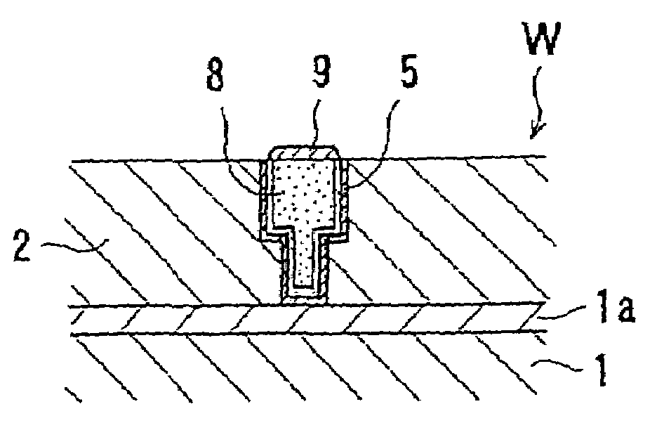
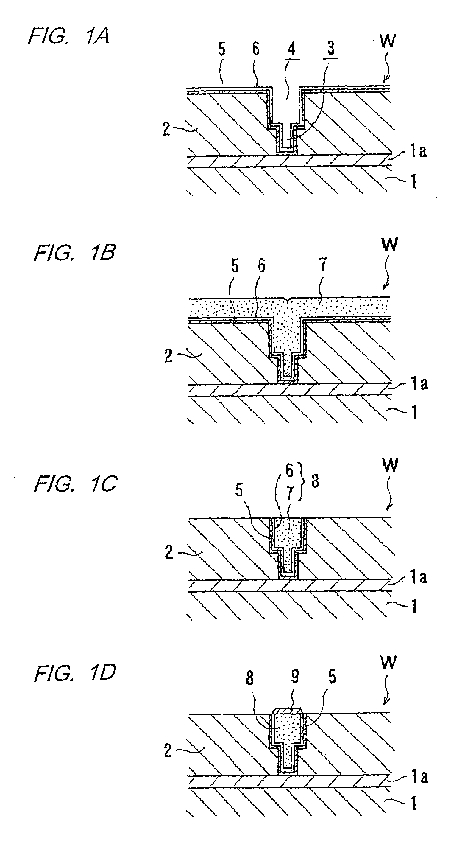
[0055]FIGS. 1A through 1D illustrate an example of forming copper interconnects in a semiconductor device. As shown in FIG. 1A, an insulating film (interlevel dielectric film) 2, such as an oxide film of SiO2 or a film of low-k material, is deposited on a conductive layer 1a on a semiconductor base 1 on which semiconductor devices are formed. Via holes 3 and interconnect trenches 4 are formed in the insulating film 2 by performing a lithography / etching technique so as to provide fine recesses ...


PUM

PropertyMeasurementUnit
electric conductivityaaaaaaaaaa
thicknessaaaaaaaaaa
thicknessaaaaaaaaaa

Abstract

A plating method is capable of depositing a plated film having excellent in-plane uniformity with respect to a thin seed layer and excellent embeddability with respect to fine damascene structures. The plating method includes: positioning an electric resistor between a conductive layer formed on at least a portion of a surface of a substrate and an anode; introducing respectively a plating solution into a space between the conductive layer and the anode on a conductive layer side, and an anode solution into a space between the conductive layer and the anode on an anode side, thereby filling the space with a plating bath composed of the plating solution and the anode solution, with the plating solution containing 25 to 75 g / L of copper ions and at least 0.4 mole / L of an organic acid or an inorganic acid, and the anode solution being of the same composition as the plating solution, or containing 0 to 75 g / L of copper ions and at most 0.6 mole / L of an organic acid or an inorganic acid; and applying a voltage between the conductive layer and the anode to plate a surface of the conductive layer.

Description

BACKGROUND OF THE INVENTION[0001]1. Field of the Invention[0002]The present invention relates to a plating method and a plating apparatus, and more particularly to a plating method and a plating apparatus used for filling a fine interconnect pattern formed in a substrate, such as a semiconductor wafer, with metal (interconnect material) such as copper so as to form interconnects.[0003]2. Description of the Related Art[0004]Recently, the so-called damascene process has been used in the art as a process of forming copper interconnects in semiconductor devices. According to the damascene process, fine interconnect recesses such as interconnect trenches in circuit patterns and via holes are formed in an insulating film (inter level dielectric film) laminated on a surface of a semiconductor wafer, and then filled with copper as an interconnect material. Thereafter, extra copper layer (plated film) is removed from the surface by a chemical mechanical polishing (CMP) process or the like to...

Claims


Application Information

Patent Timeline
Patent Type & Authority Patents(United States)
IPC IPC(8): H01L21/44C25D3/38C25D7/12H01L21/288H01L21/768
CPCC25D3/38C25D17/001H01L21/2885C25D7/123
Inventor IDE, KUNIHITOMISHIMA, KOJIKANDA, HIROYUKISUZUKI, HIDENAONOMURA, KAZUFUMI
Owner EBARA CORP
Learn More