Expansion constrained die stack

a technology of die stack and expansion restriction, which is applied in the direction of printed circuit aspects, printed circuit stress/warp reduction, basic electric elements, etc., can solve problems such as additional interference, and achieve the effects of increasing the density of components, and increasing speed

Inactive Publication Date: 2007-02-06
STABLCOR TECH
View PDF27 Cites 25 Cited by
  • Summary
  • Abstract
  • Description
  • Claims
  • Application Information

AI Technical Summary

Benefits of technology

[0006]Die stacking is a technique for mounting components on a printed wiring board that can enable an increased density of components. Increasing the density of components can enable higher speed by reducing the length of circuit traces between components, which decreases the amount of inductance and interference. Die stacking allows for various packaging types such as Multi Chip Modules (MCMs) and Chip Scale Packages (CSPs).

Problems solved by technology

A longer track can introduce additional inductance and can also result in additional interference.

Method used


Image

  • Expansion constrained die stack
  • Expansion constrained die stack
  • Expansion constrained die stack

Examples


Embodiment Construction

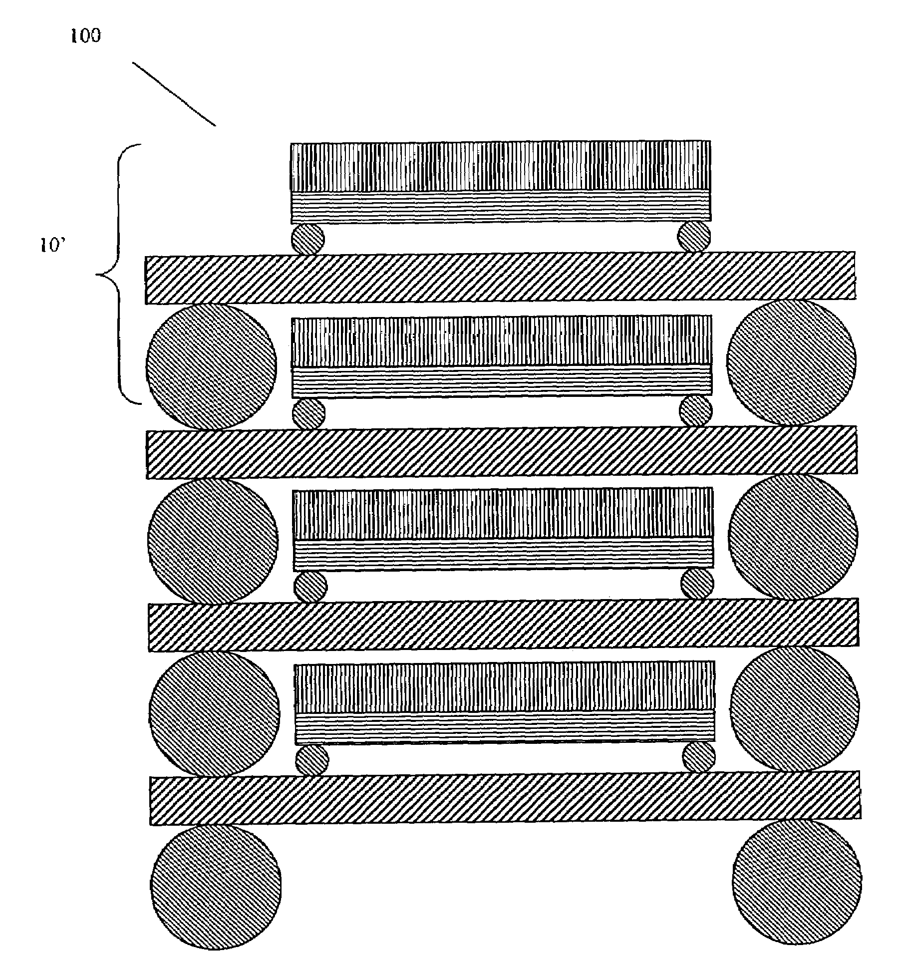
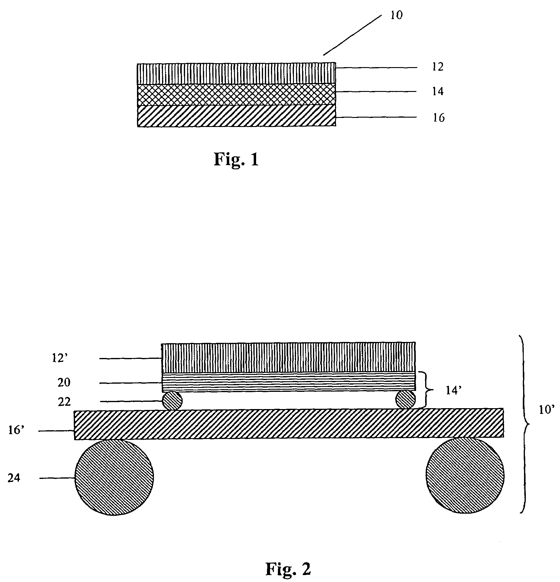
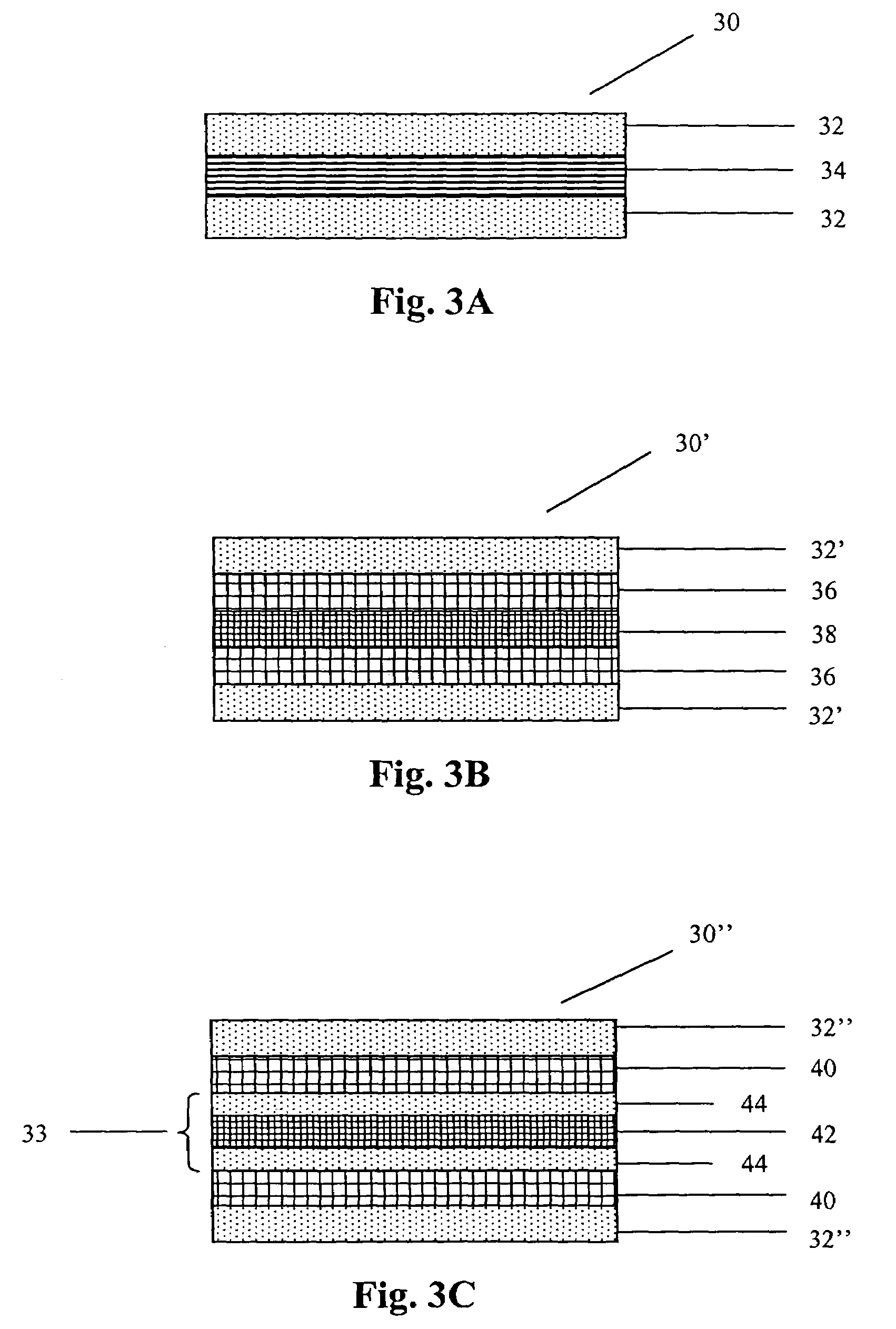
[0042]Turning now to the drawings, printed wiring board assemblies are shown that can be used to create die stacks. In one embodiment, the printed wiring board assemblies include semiconductor dies that are attached to an interposer substrate using components that can be conceptualized as an electrical connection layer. The printed wiring board assemblies can be configured with single or multiple semiconductor dies attached to one or both sides of the interposer substrate in any variety of configurations. The printed wiring board assemblies in accordance with the present invention can be layered to form die stacks. In several embodiments, intermediate substrates are used to facilitate the creation of die stacks. In another aspect of the invention, one or more die stacks in various die stack configurations can be mounted on a printed wiring board to create a die stack assembly. The use of interconnection components to connect adjacent layers in the die stack can enable the communicat...


PUM


Abstract

Structures and techniques for mounting semiconductor dies are disclosed. In one embodiment, the invention includes a stack of printed wiring board assemblies that are connected via interconnection components. At least one of the printed wiring board assemblies includes an interposer substrate having a constraining layer that includes carbon.

Description

CROSS-REFERENCE TO RELATED APPLICATIONS[0001]This application claims priority to U.S. Provisional Application No. 60 / 498,957, filed Aug. 29, 2003, the disclosure of which is incorporated herein by reference.BACKGROUND[0002]The following invention relates generally to mounting components on printed wiring boards and more specifically to using die stacks to mount components on printed wiring boards.[0003]Printed wiring boards are often used to establish electrical connections between various electronic devices. Printed wiring boards can be rigid or flexible and include a single functional layer or multiple functional layers. The length of the circuit trace connecting the electrical devices can impact on the operation of the devices. A longer track can introduce additional inductance and can also result in additional interference. Reducing the length of the path that signals must travel between components can decrease inductance and signal interference.[0004]One approach to reducing th...

Claims


Application Information

Patent Timeline
Patent Type & Authority Patents(United States)
IPC IPC(8): H01L23/02H01L23/06H01L23/34H01L23/48H01L23/52H01L23/14H01L23/492H01L23/498H01L23/538H01L25/065H01L25/10H05KH05K1/02H05K1/05H05K1/14
CPCH01L23/14H01L23/4922H01L23/49877H01L23/5385H01L25/0652H01L25/0657H01L25/105H05K1/144H01L23/145H01L2224/81138H01L2225/06513H01L2924/01078H01L2924/01079H01L2924/15311H01L2924/1532H01L2924/15331H05K1/0271H05K1/056H05K2201/0323H05K2201/068H05K2201/10734H01L2225/107H01L2924/01019H01L2225/1005H01L2224/16225
Inventor VASOYA, KALU K.MANGROLIA, BHARAT M.
Owner STABLCOR TECH
Why Eureka
Try Eureka