Al technical title is built by PatSnap Al team. It summarizes the technical point description of the patent document.
a technology of organic devices and contacts, applied in the direction of organic semiconductor devices, solid-state devices, discharge tubes/lamp details, etc., can solve the problems of low contrast and resolution, no other medium offers the speed, versatility and interactivity, and lcds operate, etc., to achieve high contrast and resolution, high reliability, and substantial transparency
Inactive Publication Date: 2007-02-06
THE TRUSTEES FOR PRINCETON UNIV
View PDF119 Cites 237 Cited by
Summary
Abstract
Description
Claims
Application Information
AI Technical Summary
This helps you quickly interpret patents by identifying the three key elements:
Problems solved by technology
Method used
Benefits of technology
[0017]It is another object of the present invention to provide a three color organic light emitting device which is extremely reliable, substantially transparent when de-energized, and relatively inexpensive to produce.
[0018]It is a further object to provide such a device which is implemented by the growth of organic materials similar to those materials used in electroluminescent diodes, to obtain an organic LED which is highly reliable, compact, efficient and requires low drive voltages for utilization in RGB displays.
Problems solved by technology
No other medium offers its speed, versatility and interactivity.
LCDs operate fairly reliably but have relatively low contrast and resolution, and require high power backlighting.
If the layers are too thin there may be lack of continuity in the film, and thicker films tend to have a high internal resistance requiring higher power operation.
These structures undoubtedly limit the charge carrier mobility across the film which, in turn, limits current and increases drive voltage.
Migration and growth of crystallites arising from the polycrystalline state is a pronounced failure mode of such devices.
Electrode contact degradation is also a pronounced failure mechanism.
The use of materials doped with fluorescent dyes to emit green or red on absorption of blue light from the blue subpixel region is less efficient than direct formation via green or red LED's.
Thus a drawback of this display is that different laterally spaced subpixel regions are required for each color emitted.
Method used
Image
Click on the blue label to locate the original text in one second.
Reading with bidirectional positioning of images and text.
Examples
Embodiment Construction
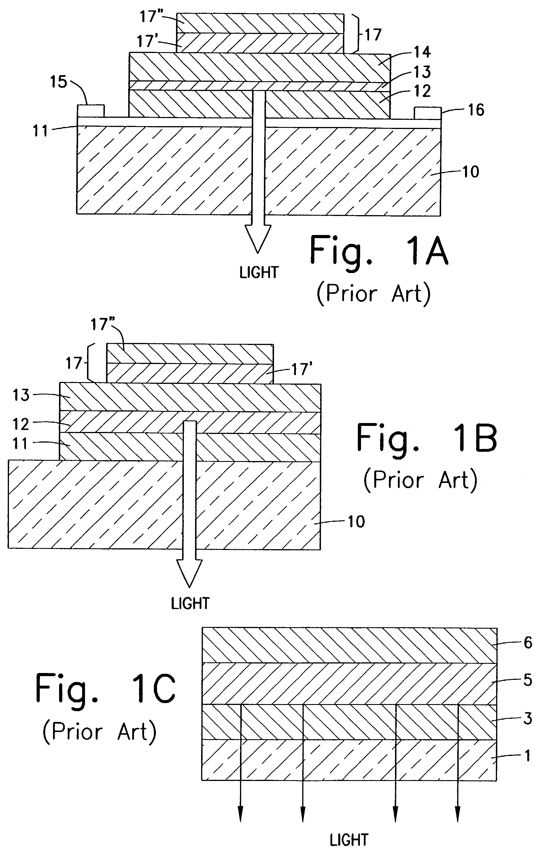
[0040]FIG. 1A has been described and is a prior art double heterostructure organic light emitting device. The basic construction of the device of FIG. 1A is used in this invention as will be described.
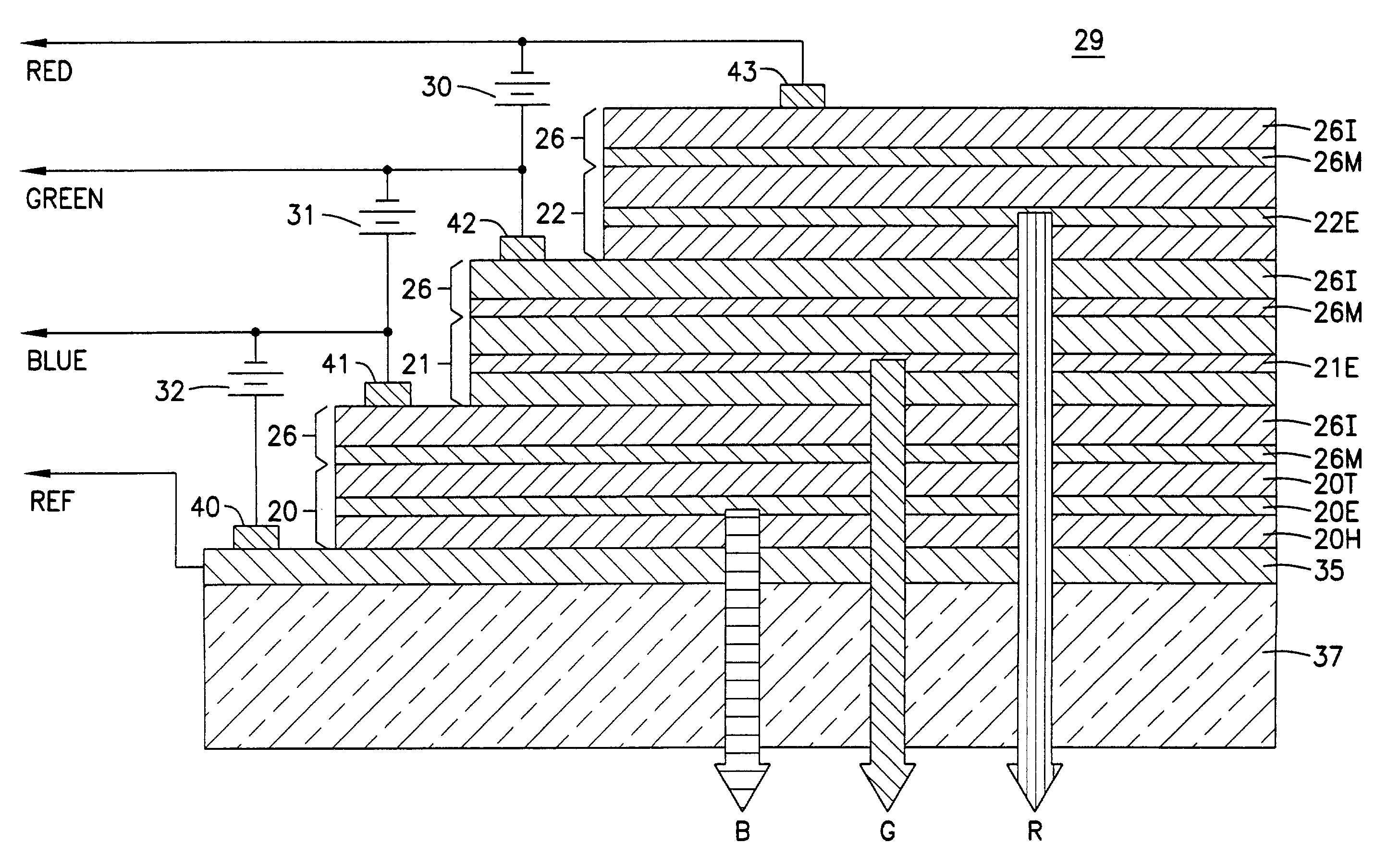
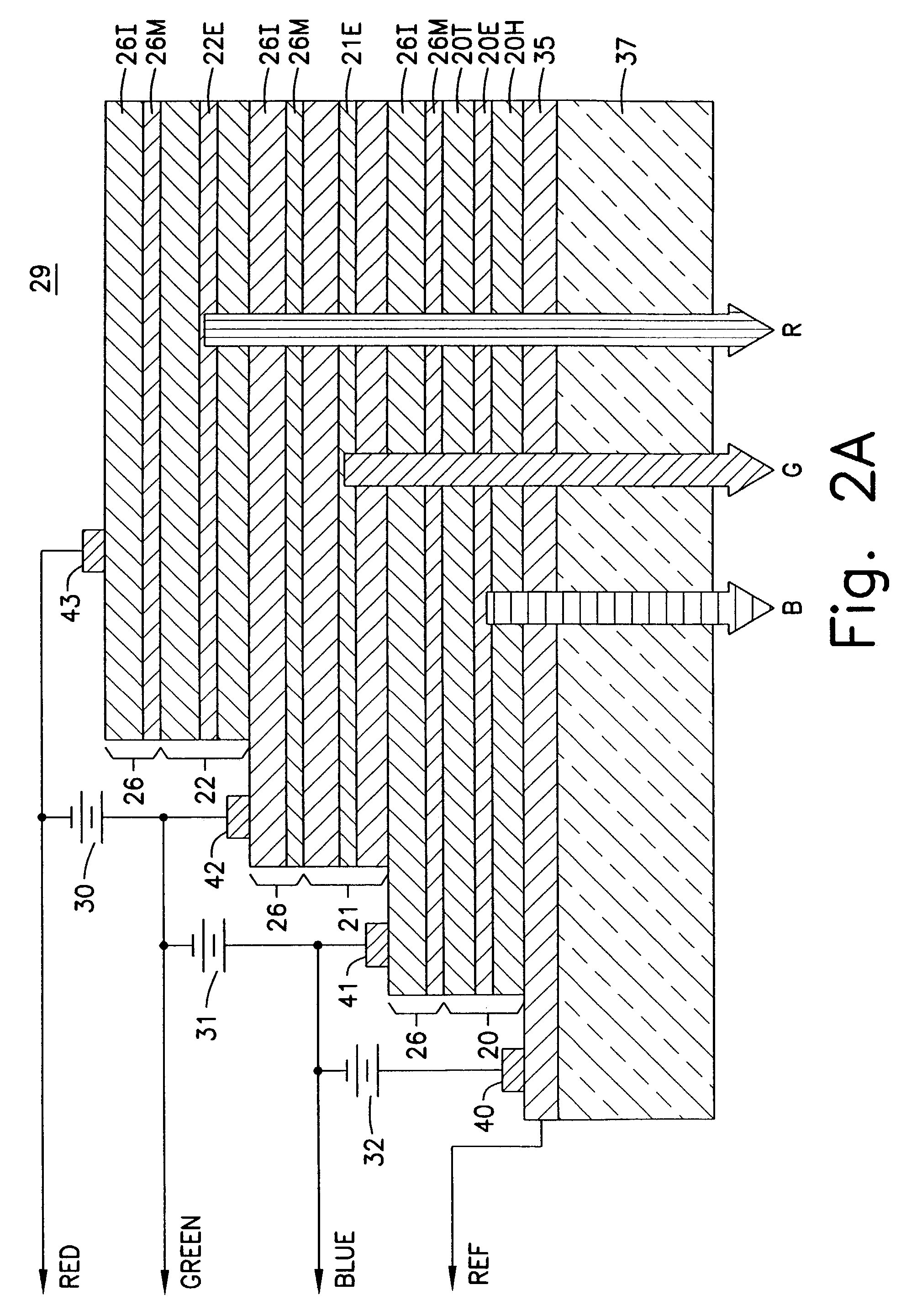
[0041]Referring to FIG. 2A, there is shown a schematic cross section of a highly compact, integrated RGB pixel structure which is implemented by grown or vacuum deposited organic layers, in one embodiment of the invention. Based on the ability to grow organic materials on a large variety of materials (including metals and ITO), one can construct a stack of LED double heterostructures (DH) designated as 20, 21 and 22, in one embodiment of the invention. For illustrative purposes, LED 20 is considered in a bottom portion of the stack, LED 21 in a middle portion of the stack, and LED 22 in a top portion of the stack, in the example of FIG. 2A. Also, the stack is shown to be vertically oriented in FIG. 2A, but the LED can be otherwise oriented. In other embodiments, a stack of single heter...
PUM
Property
Measurement
Unit
work function
aaaaa
aaaaa
thickness
aaaaa
aaaaa
thickness
aaaaa
aaaaa
Abstract
An organic light emitting device structure includes a substrate, a first electrically conductive layer formed over the substrate wherein the first electrically conductive layer has a positive polarity, and a transparent organic light emitting device formed over the first electrically conductive layer. The structure also includes a transparent electrically conductive metal layer formed over the transparent organic light emitting device wherein the metal has a work function less than 4 eV, and a second electrically conductive layer formed over the transparent electrically conductive metal layer, wherein the second electrically conductive layer has a negative polarity, and wherein the second electrically conductive layer comprises a material selected from the group consisting of a transparent electrically conductive oxide and a transparent electrically conductive polymer.
Description
[0001]This application is a continuation of U.S. application Ser. No. 09 / 468,986, filed Dec. 21, 1999, now U.S. Pat. No. 6,596,134, which is a continuation of U.S. application Ser. No. 08 / 872,560, filed Jun. 10, 1997, now U.S. Pat. No. 6,264,805, which is a divisional of U.S. application Ser. No. 08 / 613,207, filed on Mar. 6, 1996, now U.S. Pat. No. 5,703,436, which is a continuation-in-part of U.S. aplication Ser. No. 08 / 354,674, filed on Dec. 13, 1994, now U.S. Pat. No. 5,707,745.GOVERNMENT RIGHTS[0002]This invention was made with Government support under Contract No. F33615-94-1-1414 awarded by DARPA. The Government has certain fights in this invention.RESEARCH AGREEMENTS[0003]The claimed invention was made by, on behalf of, and / or in connection with one or more of the following parties to a joint university-corporation research agreement: Princeton University, The University of Southern California, and Universal Display Corporation. The agreement was in effect on and before the d...
Claims
Application Information
Patent Timeline
Application Date:The date an application was filed.
Publication Date:The date a patent or application was officially published.
First Publication Date:The earliest publication date of a patent with the same application number.
Issue Date:Publication date of the patent grant document.
PCT Entry Date:The Entry date of PCT National Phase.
Estimated Expiry Date:The statutory expiry date of a patent right according to the Patent Law, and it is the longest term of protection that the patent right can achieve without the termination of the patent right due to other reasons(Term extension factor has been taken into account ).
Invalid Date:Actual expiry date is based on effective date or publication date of legal transaction data of invalid patent.