Method of manufacturing thin quartz crystal wafer

a technology of quartz crystal wafer and manufacturing method, which is applied in the direction of piezoelectric/electrostrictive transducers, crystal growth processes, transducer types, etc., can solve the problems of low productivity and waste of material produced in the manufacturing process, and achieve the effect of reducing quartz crystal waste, high productivity and increasing productivity

Inactive Publication Date: 2007-02-13
NIHON DEMPA KOGYO CO LTD
View PDF7 Cites 59 Cited by
  • Summary
  • Abstract
  • Description
  • Claims
  • Application Information

AI Technical Summary

Benefits of technology

[0012]According to the present invention, the stealth dicing technique is applied to a quartz crystal block for manufacturing thin quartz crystal wafers with high productivity. The steps (a) and (b) may be repeatedly carried out on the quartz crystal block from which the thin quartz crystal wafer has been peeled, for thereby peeling a plurality of thin quartz crystal wafers successively from the principal surface of the quartz crystal block. According to this process, quartz crystal wastes may be reduced, and the productivity may further be increased. The principal surface of the quartz crystal block may be polished after the thin quartz crystal wafer has been peeled therefrom, and the step (a) may be carried out on the quartz crystal block. The laser beam may thus be well transmitted into the quartz crystal block, allowing the process of peeling off thin quartz crystal wafers successively from the quartz crystal block to be carried out better.
[0013]Each of the thin quartz crystal wafers thus obtained may be divided into individual crystal blanks for use in crystal units. Using such crystal blanks, crystal units can be produced inexpensively.

Problems solved by technology

Therefore, the manufacturing process produces material wastes and is low in productivity.

Method used


Image

  • Method of manufacturing thin quartz crystal wafer
  • Method of manufacturing thin quartz crystal wafer
  • Method of manufacturing thin quartz crystal wafer

Examples


Embodiment Construction

[0019]A method of manufacturing a thin quartz crystal wafer according to a preferred embodiment of the present invention will be described below.

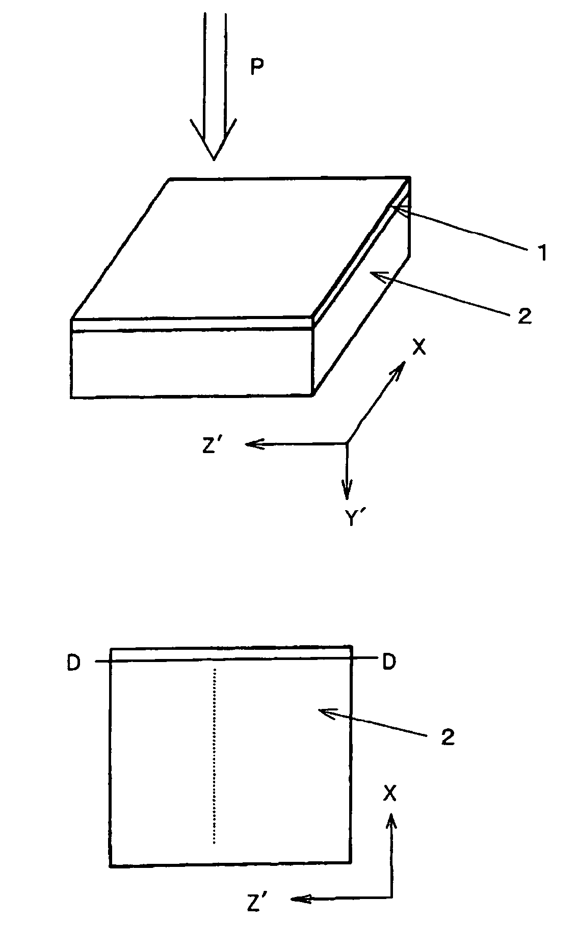
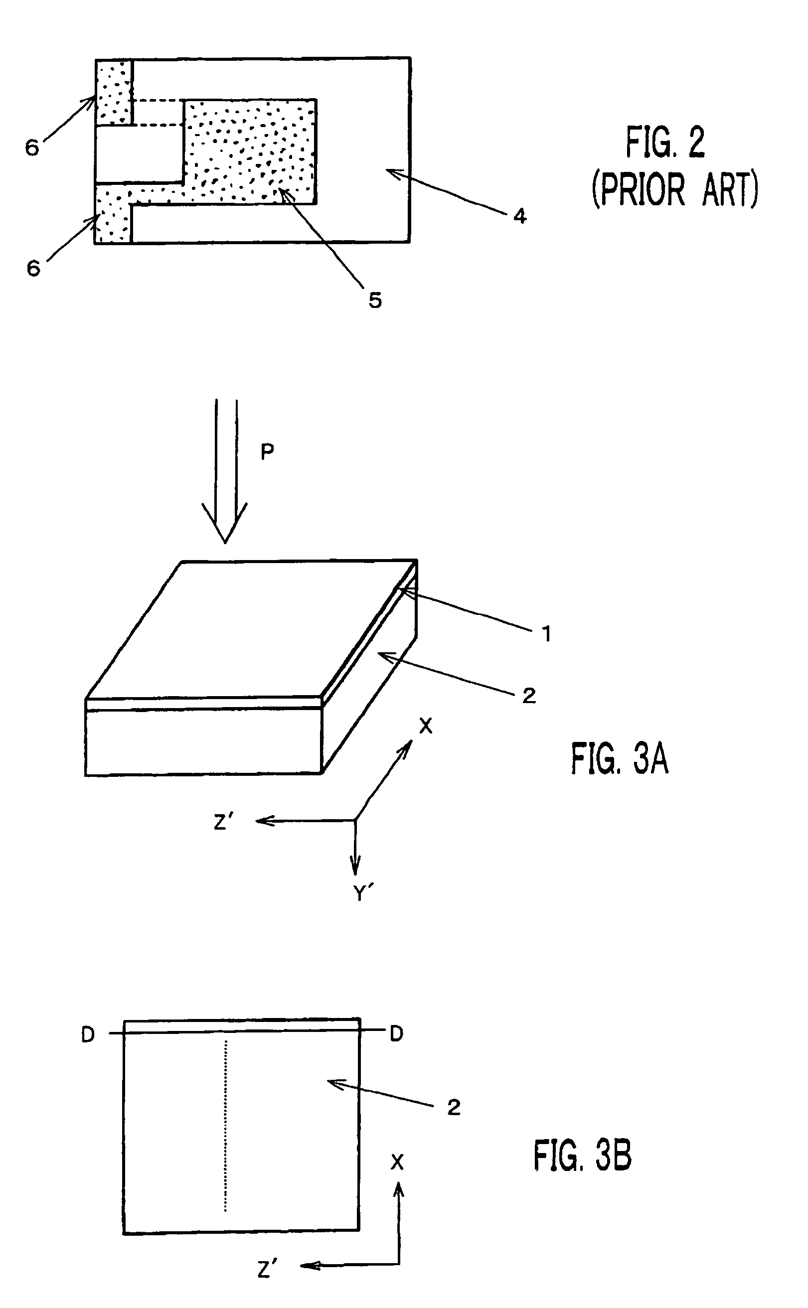
[0020]According to the embodiment, as shown in FIG. 3A, thin quartz crystal wafer 1 is cut from quartz crystal block 2 in the form of a rectangular parallelepiped having flat surfaces. AT-cut quartz crystal blanks are produced from thin quartz crystal wafer 1. As shown in FIG. 3A, quartz crystal block 2 is cut from a crystal body (not shown) of synthetic quartz crystal along X-, Y′-, and Z′-axes of quartz crystal. Specifically, quartz crystal block 2 has six surfaces including a pair of XZ′ surfaces, a pair of XY′ surfaces, and a pair of Y′Z′ surfaces. If the XZ′ surfaces of quart crystal block 2 are regarded as principal surfaces, then these principal surfaces are first polished to a mirror finish.

[0021]Then, while quartz crystal block 2 is moving in the direction of the Z′-axis, one of the principal surfaces of quartz crystal block 2 is c...


PUM

PropertyMeasurementUnit
thicknessaaaaaaaaaa
thicknessaaaaaaaaaa
thicknessaaaaaaaaaa

Abstract

A method of manufacturing a thin quartz crystal wafer from a quartz crystal block which is cut from a crystal body of synthetic quartz crystal and has a flat principal surface, comprises the steps of (a) converging a laser beam at a region in said quartz crystal block at a predetermined depth from the principal surface thereof to cause multiphoton phenomenon state, thereby breaking Si—O—Si bonds of quartz crystal in said region to form voids in said region, and (b) peeling said thin quartz crystal wafer from a body of said quartz crystal block along said voids. The above process is repeatedly performed on one quartz crystal block to peel off a plurality of thin quartz crystal wafers successively from the principal surface of the quartz crystal block. Each of the thin quartz crystal wafers is divided into individual quartz crystal blanks for making quartz crystal units.

Description

BACKGROUND OF THE INVENTION[0001]1. Field of the Invention[0002]The present invention relates to a method of manufacturing a thin quartz crystal wafer from a crystal body of synthetic quartz crystal, and more particularly to a method of manufacturing a thin quartz crystal wafer using a laser beam.[0003]2. Description of the Related Art[0004]Synthetic quartz crystal that is produced by growing quartz crystal according to hydrothermal synthesis or the like is known as a major material of electronic components typified by quartz crystal units. A quartz crystal unit comprising a quartz crystal blank cut from synthetic quartz crystal and hermetically sealed in a casing is used as a frequency control element in an oscillator or a filter. An AT-cut quartz crystal blank whose resonant frequency is inversely proportional to its thickness is widely used in such a crystal unit. A crystal blank is generally manufactured by cutting a thin quartz crystal wafer having a desired thickness. In recen...

Claims


Application Information

Patent Timeline
Patent Type & Authority Patents(United States)
IPC IPC(8): H04R31/00B28D5/00B23K26/00C30B29/18C30B33/00H03H3/02H03H9/10H03H9/19
CPCC30B29/18C30B33/00H03H3/02Y10T29/49798Y10T29/49005Y10T29/49002Y10T29/42H03H9/19
Inventor CHIBA, AKIOONO, KOZOKUROSAWA, TAMOTSU
Owner NIHON DEMPA KOGYO CO LTD
Why Eureka
Try Eureka