Phase-locked loop and delay-locked loop including differential delay cells having differential control inputs
- Summary
- Abstract
- Description
- Claims
- Application Information
AI Technical Summary
Benefits of technology
Problems solved by technology
Method used
Image
Examples
Embodiment Construction
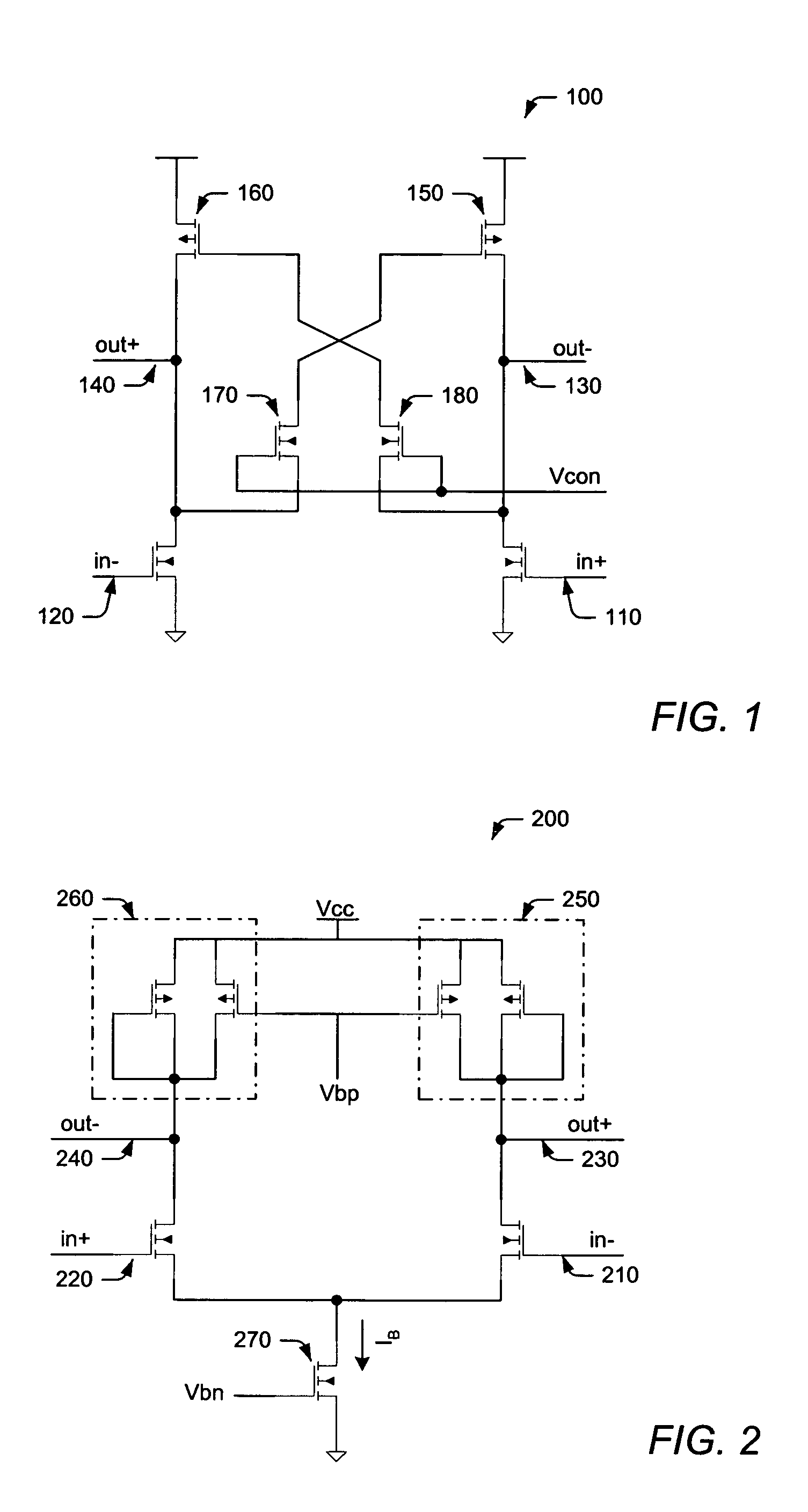
[0037]Turning now to the drawings, FIG. 1 illustrates a differential delay cell 100 having differential inputs 110, 120 and differential outputs 130, 140. In addition, delay cell 100 utilizes a pair PMOS load transistors 150, 160 to form a CMOS latch, while using cross-coupled NMOS transistors 170, 180 to control the gate voltage of PMOS transistors 150, 160, respectively. As such, cross-coupled NMOS transistors 170, 180 function to limit the strength of the CMOS latch. This mechanism is used to control the delay of cell 100 by applying a single-ended control voltage (“Vcon”) to the gate of cross-coupled transistors 170, 180. The delay time may be reduced, for example, by setting Vcon to a low value, thereby weakening the CMOS latch and increasing the output driving current through the PMOS load. Conversely, the delay time may be increased by setting Vcon to a high value, thereby enabling the CMOS latch to resist voltage switching in differential delay cell 100.
[0038]Unfortunately, ...
PUM
 Abstract
Description
Claims
Application Information


