Nonvolatile semiconductor memory having plural data storage portions for a bit line connected to memory cells

a technology of nonvolatile semiconductor memory and bit line connection, which is applied in the direction of digital storage, instruments, transistors, etc., can solve the problems of disadvantageous increase of chip area and increase of latch circuits (sram cells) on memory chips, and achieve the effect of preventing the area of the chip from extremely increasing

Inactive Publication Date: 2007-02-13
TOSHIBA MEMORY CORP
View PDF24 Cites 52 Cited by
  • Summary
  • Abstract
  • Description
  • Claims
  • Application Information

AI Technical Summary

Benefits of technology

[0065]The present invention has been made to solve the above-stated disadvantages. It is, therefore, an object of the present invention to provide a data circuit (a storage circuit temporarily storing multi-level data during program / read operations) which can prevent a chip area from extremely increasing even if data stored in a memory cell is multi-level data.

Problems solved by technology

Accordingly, if data stored in the memory cell are multi-level (n-level) data and the number of n increases, the number of latch circuits (SRAM cells) on a memory chip increases and the area of the chip disadvantageously increases.

Method used


Image

  • Nonvolatile semiconductor memory having plural data storage portions for a bit line connected to memory cells
  • Nonvolatile semiconductor memory having plural data storage portions for a bit line connected to memory cells
  • Nonvolatile semiconductor memory having plural data storage portions for a bit line connected to memory cells

Examples


Embodiment Construction

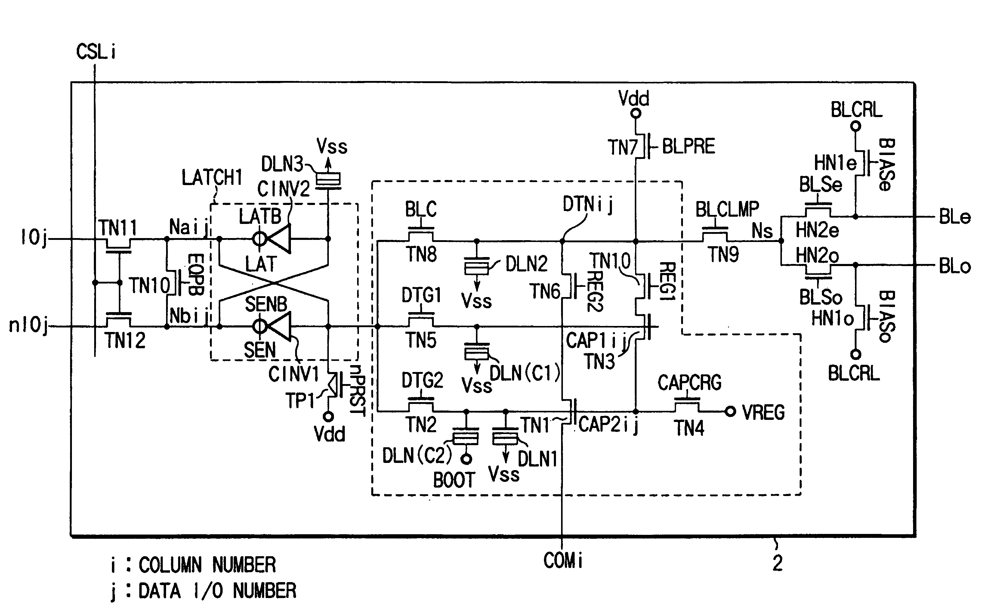
[0147]A nonvolatile semiconductor memory of the present invention will be described-below in detail with reference to the accompanying drawings.

[0148][Preconditions]

[0149]First, to facilitate understanding the description to be given below, preconditions will be specified as follows. It is noted that these preconditions are intended to facilitate understanding the description only and that the present invention is realized on conditions other than these preconditions.

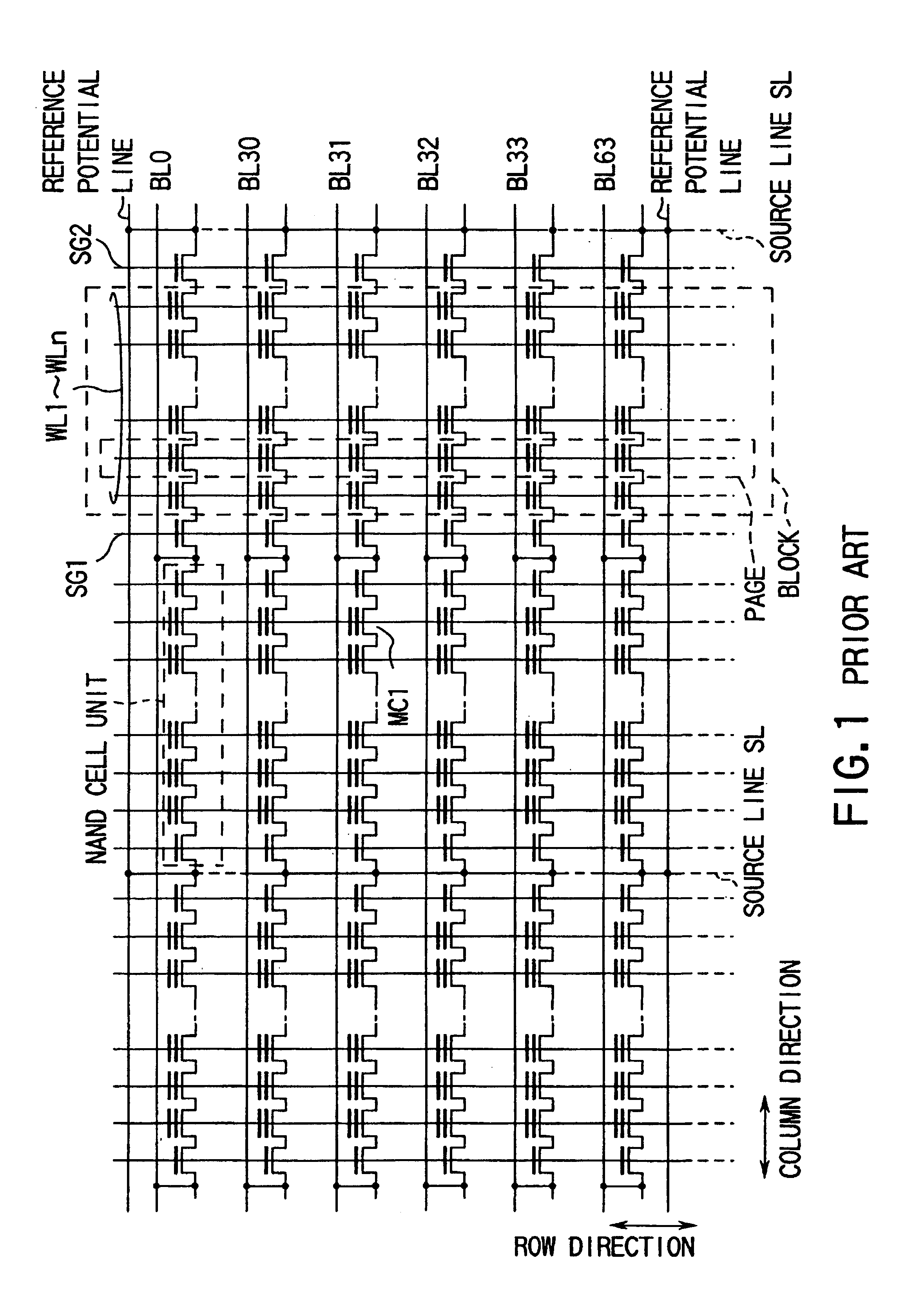
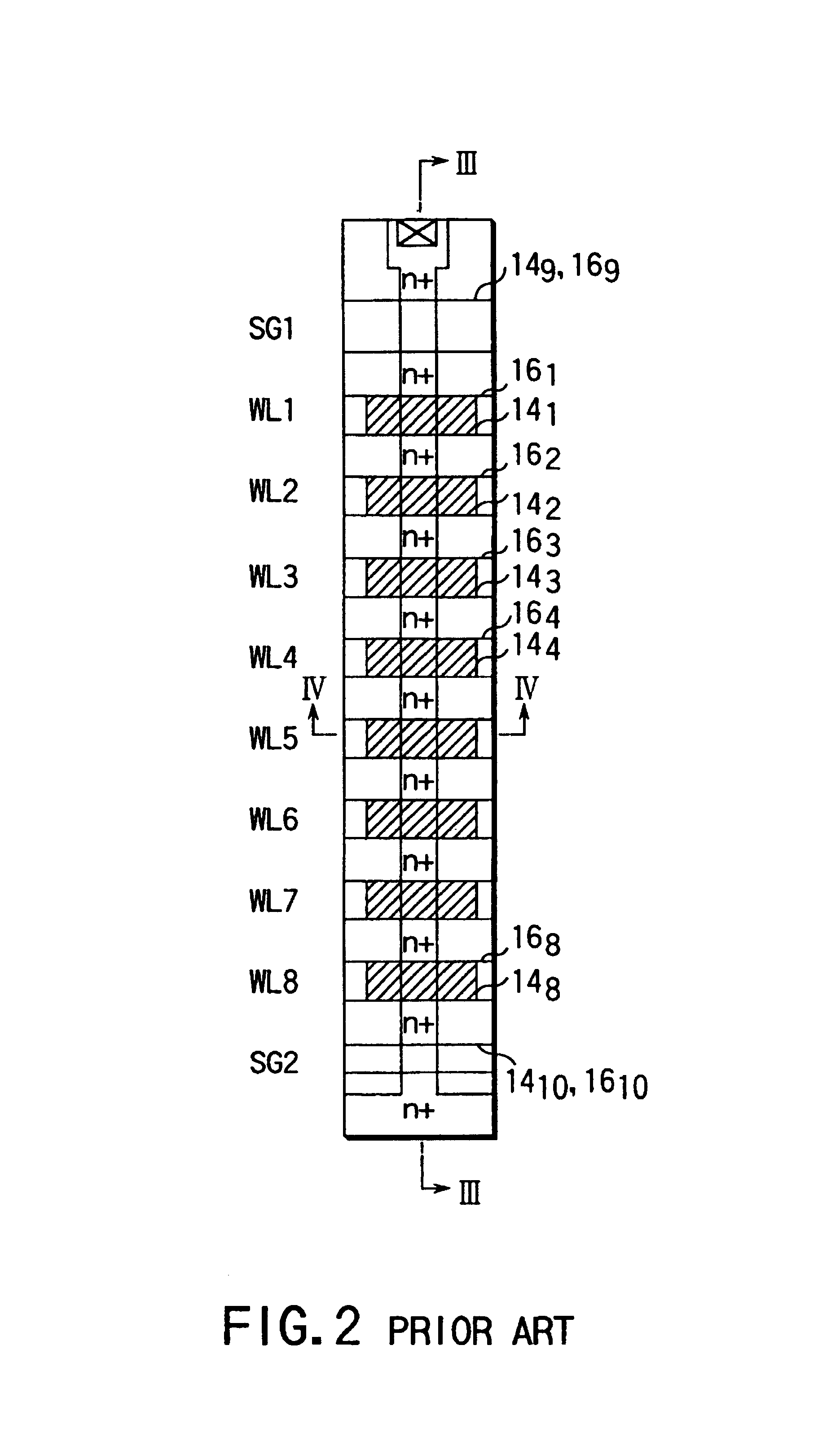
[0150]The present invention is directed to a nonvolatile semiconductor memory for storing n-level data, where n is a natural number of not lower than 3. In the following embodiments, a four-level NAND cell type EEPROM will be described to represent such nonvolatile semiconductor memories.

[0151]It is assumed that four-level data, “00”, “01”, “10” and “11”, are stored in a memory cell. It is also assumed that a state in which the threshold voltage of the memory cell is the lowest (e.g., a threshold voltage is negative) is...


PUM


Abstract

Data having three values or more is stored in a memory cell in a nonvolatile manner. A data circuit has a plurality of storage circuits. One of the plurality of storage circuits is a latch circuit. Another one of the plurality of storage circuits is a capacitor. The latch circuit and the capacitor function to temporarily store program / read data having two bits or more. Data held by the capacitor is refreshed using the latch circuit if data variation due to leakage causes a program. As a result, the data circuit does not become large in size even if multi-level data is used.

Description

[0001]This application is a Divisional of U.S. application Ser. No. 09 / 667,610 filed on Sep. 22, 2000 now U.S. Pat. No. 6,373,746 B1, hereby incorporated by reference as to its entirety.CROSS-REFERENCE TO RELATED APPLICATION[0002]This application is based on and claims the benefit of priority from the prior Japanese Patent Applications No. 11-275327, filed Sep. 28, 1999; and No. 11-345299, filed Dec. 3, 1999, the entire contents of which are incorporated herein by reference.BACKGROUND OF THE INVENTION[0003]The present invention relates to a nonvolatile semiconductor memory and particularly relates to a nonvolatile semiconductor memory used as a Multi-level NAND cell type EEPROM, e.g., a four-level NAND cell type EEPROM.[0004]There is known, as one of nonvolatile semiconductor memories, an NAND cell type EEPROM. This EEPROM has a memory cell array consisting of a plurality of NAND cell units. Each of the NAND cell units consists of a plurality of memory cells connected in series and ...

Claims


Application Information

Patent Timeline
Patent Type & Authority Patents(United States)
IPC IPC(8): G11C16/06G11C16/04G11C7/10G11C11/56G11C16/00G11C16/02H01L21/8247H01L27/115H01L29/788H01L29/792
CPCG11C7/1051G11C11/5628G11C11/5642G11C16/0483G11C16/12G11C16/24G11C16/3418G11C16/3431G11C16/3445G11C16/3459G11C11/5621G11C2216/14G11C16/08G11C2211/5621G11C2211/5642G11C2211/5643G11C2211/5649G11C2211/565G11C16/00
Inventor TAKEUCHI, KENTANAKA, TOMOHARUSHIBATA, NOBORU
Owner TOSHIBA MEMORY CORP
Why Eureka
Try Eureka