Far infrared photoconductor array

a photoconductor array and infrared radiation technology, applied in the field of infrared radiation sensing, can solve the problems of inefficient interfacing of the detecting array with the readout electronics, the inability to develop a sensing device that detects all wavelengths of radiation from the electromagnetic spectrum, and the inability to meet the requirements of the measurement device, so as to achieve significant reduction of signal contamination

Inactive Publication Date: 2007-02-20
TECHNO SCI
View PDF8 Cites 21 Cited by
  • Summary
  • Abstract
  • Description
  • Claims
  • Application Information

AI Technical Summary

Benefits of technology

[0014]A hybrid photoconductor array enables the detection of far infrared radiation without significant interference from the problems described above. An embodiment of the photoconductor array places a blocking layer in between the detecting layer and the readout layer, significantly reducing signal contamination generated by detector heating and readout glow. The blocking layer advantageously provides an electrical connection between the detecting layer and the readout layer. An embodiment provides the blocking layer with conductive vias for directing electrical signals from the detecting layer to the readout layer.

Problems solved by technology

Development of a sensing device that detects all wavelengths of radiation from the electromagnetic spectrum can be quite daunting due to the size and complexity of such a device.
The challenge of efficiently transferring information (in the form of electronic signals) from the detecting medium to the readout medium has confounded sensing device manufacturers for decades.
However, the extreme size of the detecting and readout media, and, subsequently, the large number of pixels and unit cells to be connected, render wire bonding an inefficient means for interfacing the detecting array with the readout electronics.
Several other challenges also plague the far infrared sensing device community, including the inherent temperature increase of the sensing media, the inherent radiant glow from the readout multiplexer, and a possible thermal mismatch between the sensing material and the readout material.
However, for far infrared detection, where incoming radiation is substantially less energetic than near infrared radiation and the detectors need to operate in much lower temperatures, readout glow and detector heating become problematic.
Any stray light reaching the detecting surface due to glow from the readout multiplexer will compromise detector performance.
In addition, the heat generated by the readout affects the performance of the detector array by raising its temperature.
This, in turn, causes an increase in excess dark current, thus resulting in the degradation of detector performance.
In the case that the detecting media and readout media are constructed from different materials, a thermal mismatch is created.
Another difficulty that arises when detecting radiant energy of any particular wavelength relates to the presence of optical crosstalk between adjacent pixels on the surface of a detecting array.
However, this approach to eliminating optical crosstalk is not conducive for implementation on large surface area arrays, like those needed for far infrared detection, due to the increase in processing costs for cutting grooves over such a large area.
Furthermore, another significant challenge facing far infrared sensor manufacturers involves maintaining a stable operating voltage for the detecting media during the time that the detecting media waits for its signal to be integrated by the readout media.
When the overall voltage (or bias) of the detecting media becomes unstable, or debiased, a significant limitation in detector efficiency is encountered.

Method used


Image

  • Far infrared photoconductor array
  • Far infrared photoconductor array
  • Far infrared photoconductor array

Examples


Embodiment Construction

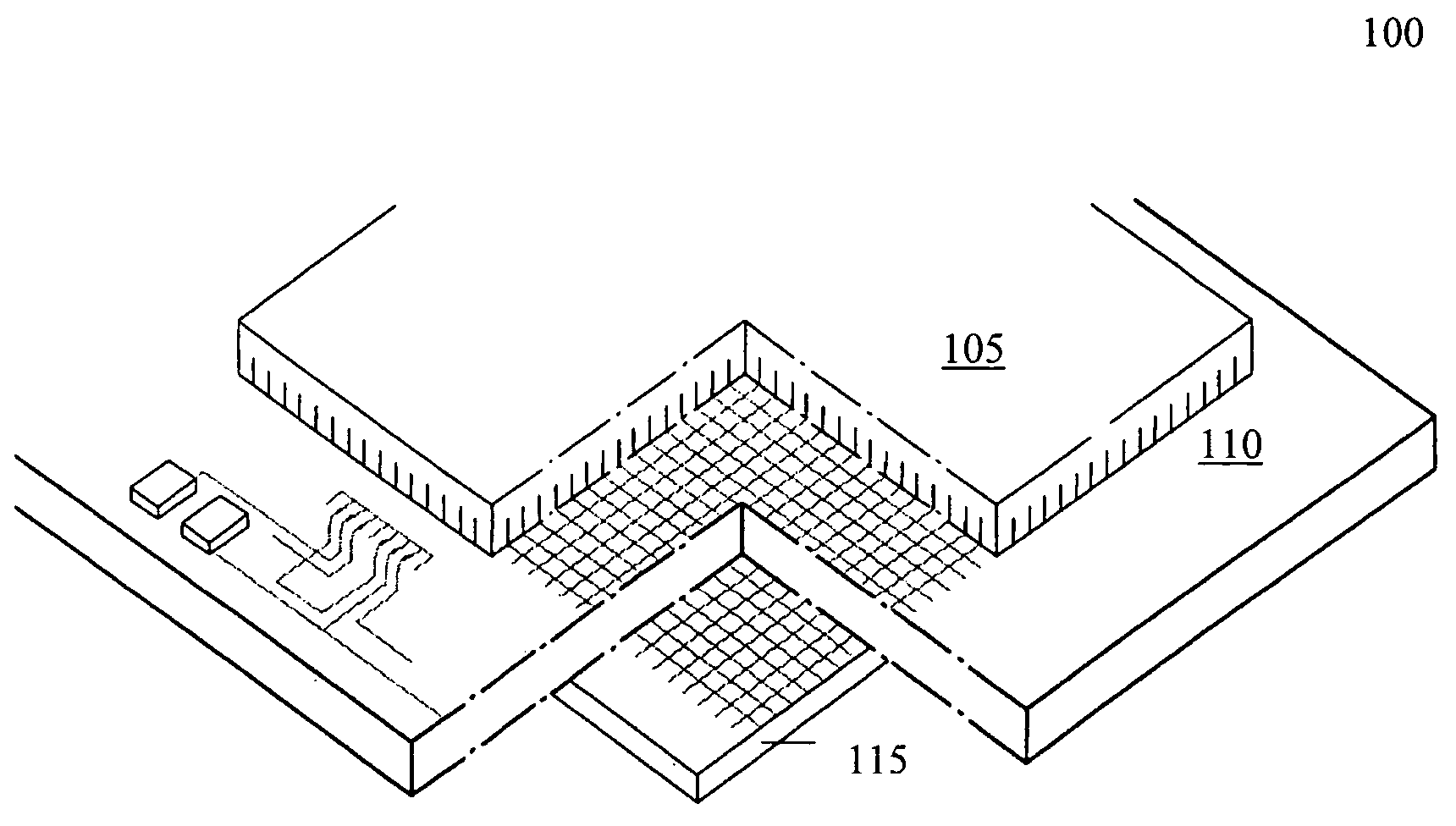
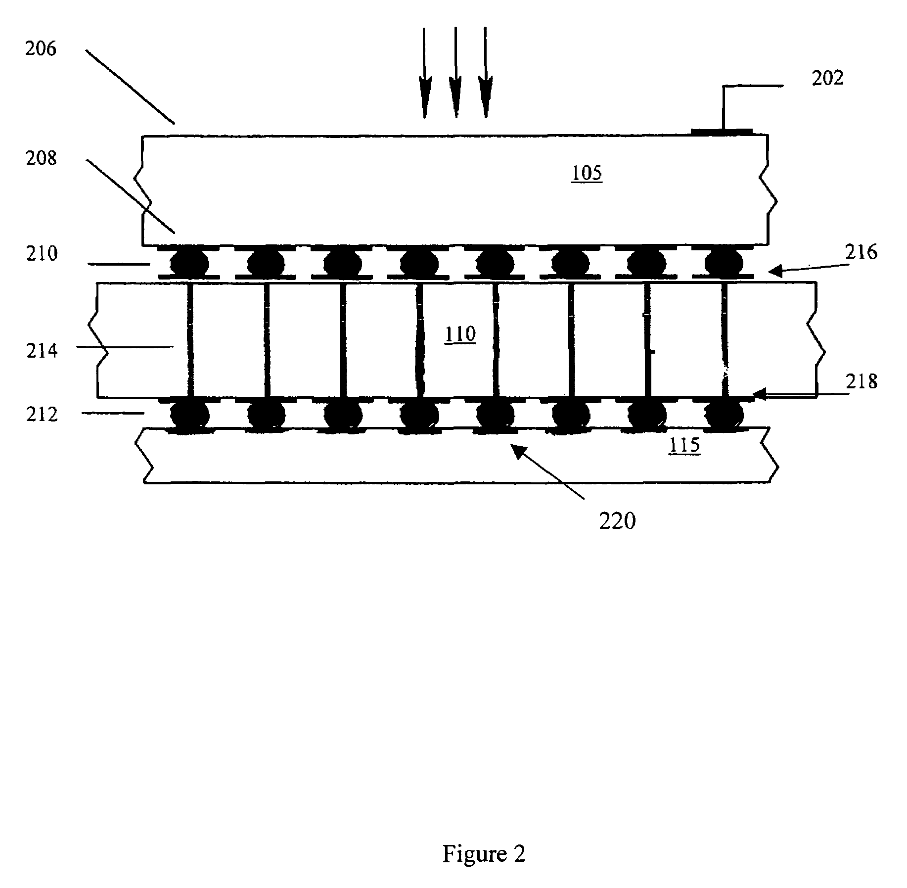
[0018]FIG. 1 illustrates a far infrared (IR) photoconductor array 100, according to one embodiment of the present invention. Photoconductor array 100 is designed such that a blocking layer 110 is sandwiched between a detecting layer 105 and a readout layer 115. The design of photoconductor array 100 provides superior protection against readout glow by having the blocking layer 110 restrict the glow from reaching the detecting layer 105.

[0019]Detecting layer 105 converts radiant energy, particularly far infrared radiation, into electrical signals containing information about the incoming radiation that are processed by readout layer 115 and subsequently analyzed by a computer-based micro-processing device. In addition to blocking the glow from the readout layer 115 from reaching detecting layer 105, the blocking layer 110 provides an effective electrical conduit between detecting layer 105 and readout layer 115 for transferring electrical signals. Readout layer 115 specifically conve...


PUM


Abstract

Fabrication of far infrared photoconductor arrays, especially for low background astronomy, is particularly challenging due to arrays' relatively large pixel size, susceptibility to stray radiation, and the requirement for low bias levels. A hybrid-far infrared photoconductor array as presented, provides a system and method for the development of large-format far IR arrays. The hybrid-far infrared array is provided with a blocking layer, situated in between a detecting layer and a readout layer, which allows detection of far infrared signals without complications based on readout glow. In particular, the readout glow, detector heating, and thermal mismatch between the readout and the detecting layer are addressed by careful selection of the materials for the blocking layer. The blocking layer is provided with an array of conductive vias passing through the bulk of the blocking layer in order to efficiently transmit electrical signals between the detecting layer and the readout layer.

Description

CROSS-REFERENCE TO RELATED APPLICATIONS[0001]This application claims the benefit of U.S. Provisional Application No. 60 / 546,700, filed Feb. 20, 2004, which is incorporated by reference herein in its entirety.BACKGROUND OF THE INVENTION[0002]1. Field of Invention[0003]This invention pertains, in general, to sensing far-infrared radiation, and in particular, to a photoconductor array for sensing radiation in the far infrared region of the electromagnetic spectrum.[0004]2. Description of the Background Art[0005]In general, sensing devices are designed to detect radiant energy found in certain regions of the electromagnetic spectrum. Development of a sensing device that detects all wavelengths of radiation from the electromagnetic spectrum can be quite daunting due to the size and complexity of such a device. Therefore, sensing device manufactures have produced devices that are sensitive to certain discrete regions of radiant energy, including far ultraviolet, near ultraviolet, visible,...

Claims


Application Information

Patent Timeline
Patent Type & Authority Patents(United States)
IPC IPC(8): G01T1/18
CPCH01L27/14603H01L27/14634H01L27/1467H01L27/1469H01L27/1463H01L2924/13091H01L2224/16225H01L2924/15311H01L2924/00H01L2224/05573H01L2224/05624H01L2224/05644H01L2224/05647H01L2924/351H01L2924/00014
Inventor FARHOOMAND, JAM
Owner TECHNO SCI
Why Eureka
Try Eureka