Ferroelectric capacitor with parallel resistance for ferroelectric memory

a ferroelectric memory and capacitor technology, applied in capacitors, semiconductor devices, semiconductor/solid-state device details, etc., can solve the problems of unfavorable memory access operations, and incorrect data to be read out of the cell, so as to reduce the charge or discharging of the storage node, inhibit the accumulation or charge loss, and significantly disrupt memory access operations.

Active Publication Date: 2007-02-20
TEXAS INSTR INC
View PDF39 Cites 32 Cited by
  • Summary
  • Abstract
  • Description
  • Claims
  • Application Information

AI Technical Summary

Benefits of technology

[0009]The present invention relates to the ferroelectric memory cells and the fabrication thereof, wherein individual ferroelectric memory cells are provided with a resistance in parallel with a ferroelectric memory cell capacitor in order to facilitate discharging of unwanted storage node voltage buildup in the memory cell caused by leaky cell transistors, while allowing normal read, write, and restore memory access operations. The invention may be advantageously employed to ensure read / write reliability in semiconductor devices employing ferroelectric memory cells, without addition of extra circuitry, without increasing the area of the memory cells, and without increasing memory access times. In addition, the invention provides for integration of the cell resistor into the ferroelectric cell capacitor structure, by which scaling efforts can continue without adding to the memory cell area.
[0011]The memory cell further comprises a cell resistor that is integral to the ferroelectric capacitor structure, where the cell resistor is in contact with the first and second electrodes and provides a resistance between the cell storage node and the cell plateline node that inhibits charge accumulation or charge loss at the cell storage node when the cell is not being accessed without significantly disrupting memory access operations when the cell is being accessed. In one example, the cell resistor provides a resistance of about 20 MOHMS or more and about 100 MOHMS or less between the cell storage node and the cell plateline node. The cell resistor may also advantageously provide a substantially linear I-V characteristic.
[0012]In one implementation, the cell resistor comprises an encapsulation layer extending between the first and second electrodes, that provides the parallel resistance between the cell storage node and the cell plateline node. The encapsulation layer may also serve as a hydrogen diffusion barrier that extends along sidewall portions of the electrodes and the ferroelectric material, and may be any suitable resistive material, such as doped aluminum oxide, for example, titanium aluminum nitride (TiAlN) or titanium aluminum oxynitride (TiAlON). In another exemplary implementation, the cell resistor is integral to the ferroelectric material, for example, by controlling the lead content of PZT ferroelectric material to include excess Pb mole fractions of about 10 percent or more and about 30 percent or less, and / or by providing doped PZT material to achieve a resistance between the capacitor electrodes that mitigates charging or discharging of the storage node when the cell transistor is off while allowing normal read, restore, and / or write operation when the cell is accessed.

Problems solved by technology

Any excess charge at the storage node of the cell, however, may disrupt or disturb the sensing of the stored data, and in some cases may cause incorrect data to be read out of the cell.
In particular, leaky cell transistors may cause unwanted charging or discharging of the cell storage node, sometimes referred to as storage node disturbance.
One possible cause of storage node disturbances occurs where the cell is not selected for a read or write access (e.g., the associated wordline is low and the transistor is theoretically off), and the cell does not receive a plateline pulse.
For example, where the data on the bitline is a “1” (e.g., the bitline is at a high voltage), leakage through the cell transistor may cause charge buildup at the storage node, thereby increasing the voltage across the cell capacitor.
Even while reading a “0” data, the voltage on the bitline can rise above 0 V, resulting in a rise or gain in storage node voltage for the cell.
Another cause may occur where plateline drivers are shared among selected and non-selected rows, wherein leakage through the non-selected cell transistors can result in storage node voltage changes when a plateline pulse is applied to the non-selected cell capacitors.
Moreover, repeated accesses to other cells may cause this acquired charge to increase over time, wherein the storage node voltage rises.
Furthermore, such storage node disturbances may be worsened through wordline coupling that temporarily raises the wordline voltage while a different (adjacent) row is being accessed.
However, these approaches require extra circuitry thus increasing the chip area occupied by the memory cells and associated circuitry, and may increase the device power consumption and the time required for a memory access operation.

Method used


Image

  • Ferroelectric capacitor with parallel resistance for ferroelectric memory
  • Ferroelectric capacitor with parallel resistance for ferroelectric memory
  • Ferroelectric capacitor with parallel resistance for ferroelectric memory

Examples


Embodiment Construction

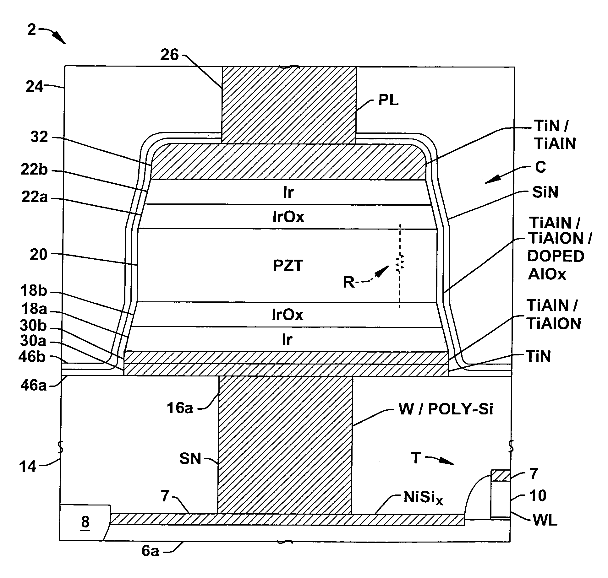
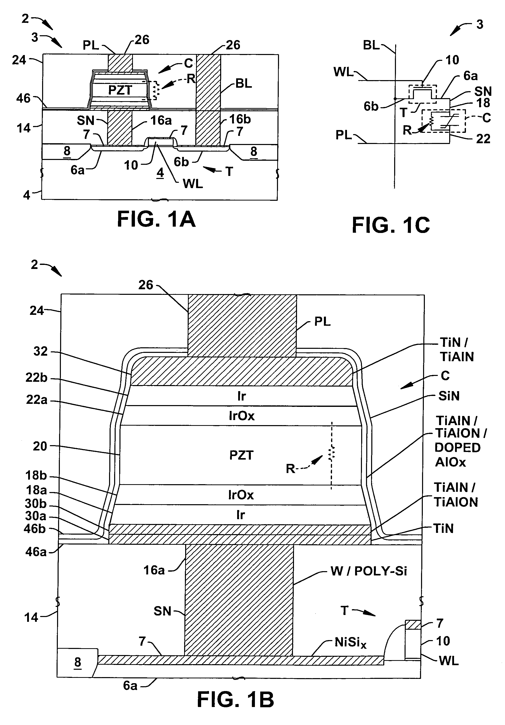
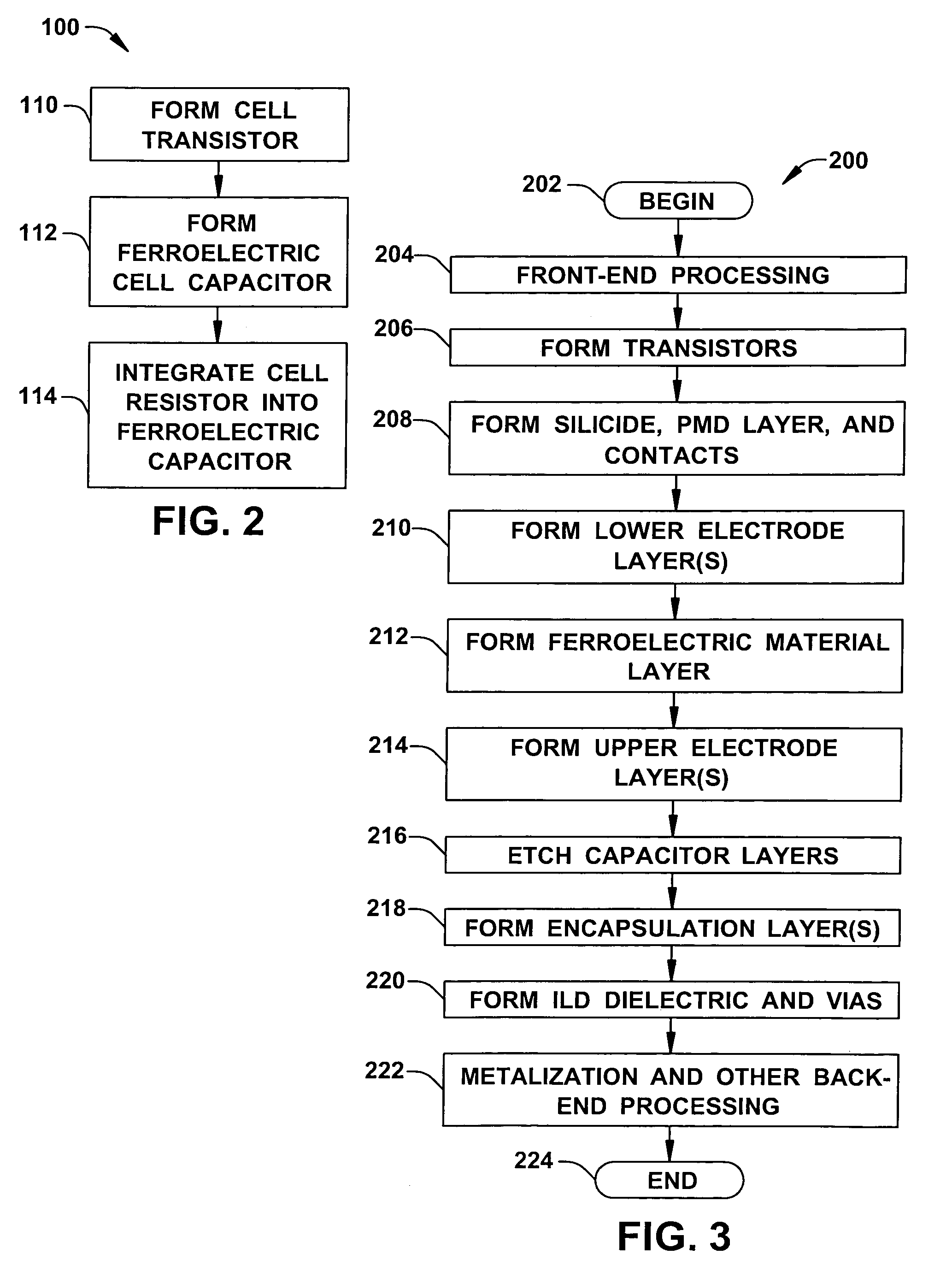
[0026]The present invention will now be described with reference to the attached drawing figures, wherein like reference numerals are used to refer to like elements throughout. The invention relates to the provision of a memory cell with a parallel resistance integrated into a ferroelectric cell capacitor stack structure, by which the adverse effects (e.g., disturb voltage) of leaky memory cell access transistors may be mitigated in semiconductor devices employing ferroelectric memory. The invention may be carried out in any type of semiconductor device, for example, devices having memory cells with ferroelectric cell capacitors or other devices, such as integrated circuits in which ferroelectric capacitors are used. The various aspects and advantages of the invention are hereinafter illustrated and described in conjunction with the drawings, wherein the illustrated structures are not necessarily drawn to scale.

[0027]FIGS. 1A–1C illustrate an exemplary ferroelectric memory cell 3 (e...


PUM


Abstract

Ferroelectric memory cells (3) are presented, in which a cell resistor (R) is integrated into the cell capacitor (C) to inhibit charge accumulation or charge loss at the cell storage node (SN) when the cell (3) is not being accessed while avoiding significant disruption of memory cell access operations. Methods (100, 200) are provided for fabricating ferroelectric memory cells (3) and ferroelectric capacitors (C), in which a parallel resistance (R) is integrated in the capacitor ferroelectric material (20) or in an encapsulation layer (46) formed over the patterned capacitor structure (C).

Description

FIELD OF INVENTION[0001]The present invention relates generally to semiconductor devices and more particularly to methods for fabricating ferroelectric capacitors with a parallel resistance.BACKGROUND OF THE INVENTION[0002]Memory systems are used for storage of data, program code, and / or other information in many electronic products, such as personal computer systems, embedded processor-based systems, video image processing circuits, portable phones, and the like. Ferroelectric memory, sometimes referred to as “FRAM” or “FERAM”, is a non-volatile form of memory commonly organized in single-transistor, single-capacitor (1T1C) or two-transistor, two-capacitor (2T2C) cell configurations, in which each memory cell includes one or more access transistors and one or more cell capacitors formed using ferroelectric dielectric material. The non-volatility of an FERAM memory cell results from a bi-stable or multi-stable characteristic of the ferroelectric dielectric material in the cell capac...

Claims


Application Information

Patent Timeline
Patent Type & Authority Patents(United States)
IPC IPC(8): H01L21/331H01L29/768
CPCH01L27/11502H01L27/11507H01L28/75H01L28/55H01L28/65H01L28/20H10B53/30H10B53/00
Inventor ELIASON, JARROD RANDALLFOX, GLEN R.BAILEY, RICHARD A.
Owner TEXAS INSTR INC
Why Eureka
Try Eureka