Light emitting device and element substrate

a technology elements, which is applied in the field of light emitting devices, can solve the problems of difficult optimization of difficult to optimize the manufacturing process of transistors, and difficulty in observing luminance decay due to degradation of light emitting materials, so as to prevent the current supplied to the light emitting element from easily fluctuating without increasing the storage capacity of capacitors, and suppress the off-current of transistors.

Inactive Publication Date: 2007-02-20
SEMICON ENERGY LAB CO LTD
View PDF5 Cites 15 Cited by
  • Summary
  • Abstract
  • Description
  • Claims
  • Application Information

AI Technical Summary

Benefits of technology

[0017]Therefore, it is possible to prevent current supplied to the light emitting element from varying easily without increasing the storage capacity of the capacitor which is disposed between the gate and source of the transistor or optimizing a manufacturing process of a transistor so as to suppress OFF-current of the transistor for controlling a video signal input to a pixel low. Thus, cause of variations is reduced and the image quality is thus enhanced to a great extent.
[0018]Also, by operating the driving transistor in a saturation region, its drain current is maintained relativel

Problems solved by technology

As an obstruction to the practical application of the light emitting device, a luminance decay due to degradation of light emitting materials can be noted.
Therefore, when a gray scale differs among pixels in each displayed image, the rate of degradation of the light emitting elements vary among pixels, leading to v

Method used


Image

  • Light emitting device and element substrate
  • Light emitting device and element substrate
  • Light emitting device and element substrate

Examples


embodiment mode 1

[0041]Described in this embodiment mode is a pixel of the light emitting device of the invention as an example.

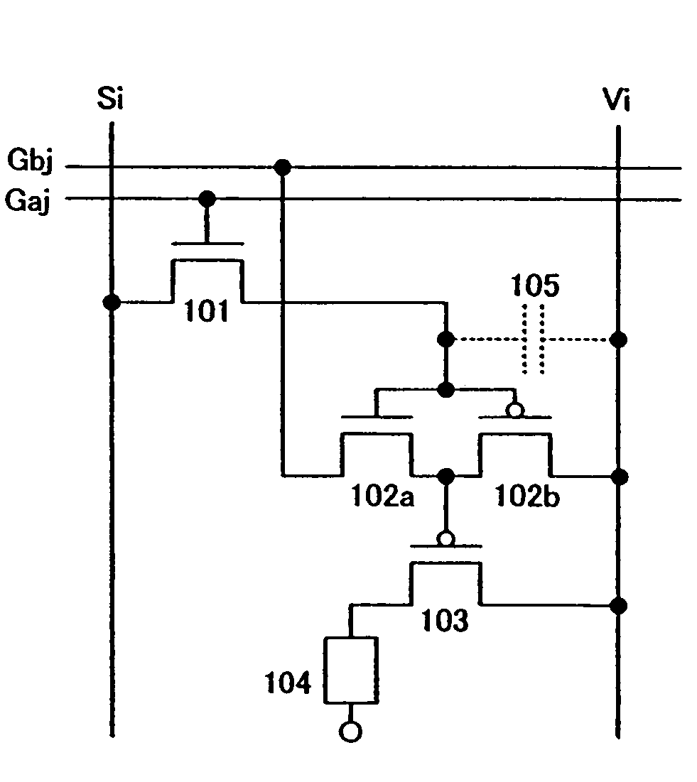
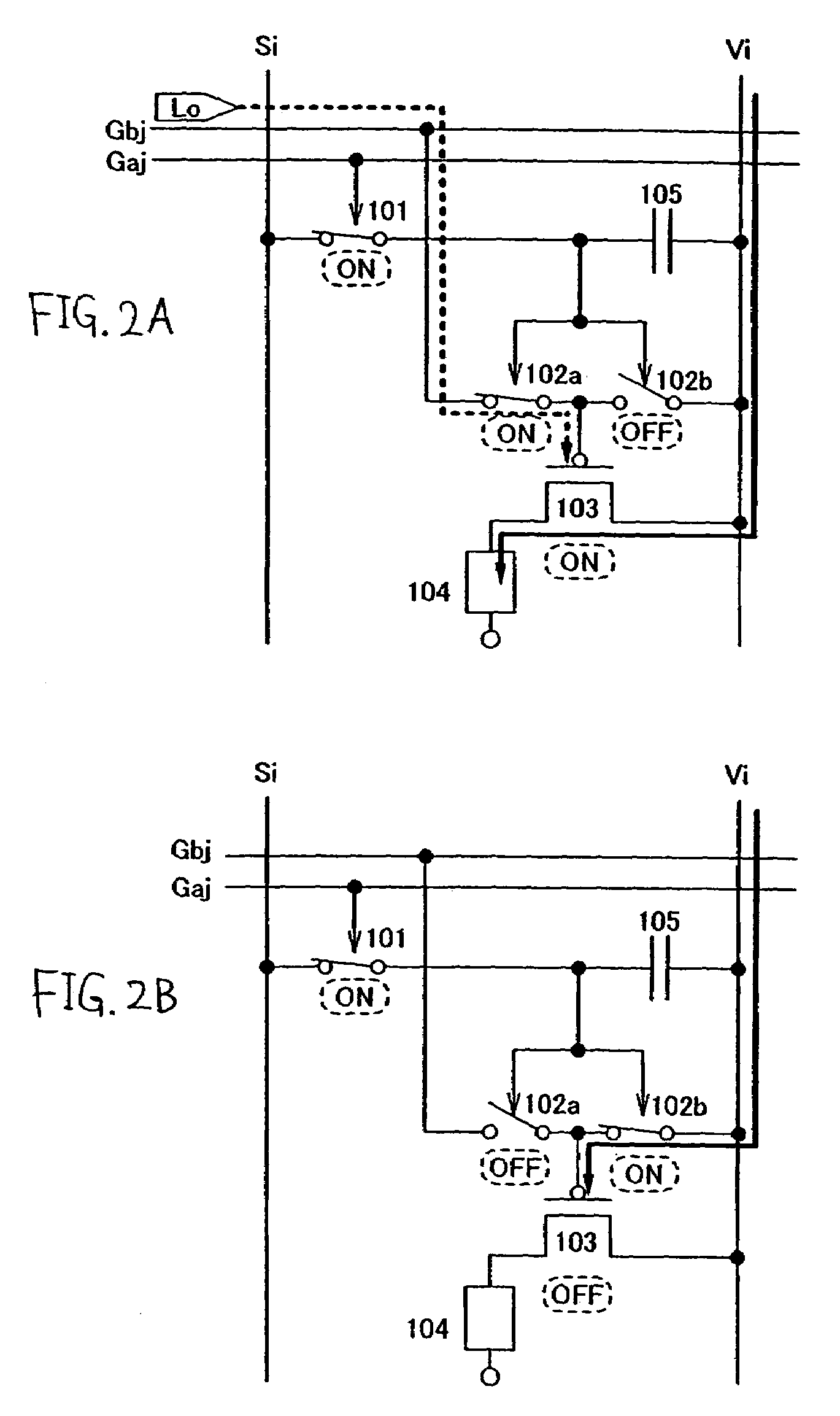
[0042]FIG. 1 shows a circuit diagram of a pixel of this embodiment mode. The pixel includes a switching transistor 101, a first current controlling transistor 102a, a second current controlling transistor 102b, a driving transistor 103, a light emitting element 104, and a capacitor 105. It should be noted that the capacitor 105 is not necessarily disposed in the pixel of the light emitting device according to the invention.

[0043]The gate of the switching transistor 101 is connected to a first scan line Gaj (j=1 to y), and either the source or the drain thereof is connected to a signal line Si (i=1 to x) and the other is connected to each gate of the first and second current controlling transistors 102a and 102b. The switching transistor 101 may be either an N-channel transistor or a P-channel transistor.

[0044]Either of the first current controlling transistor 102a or the se...

embodiment mode 2

[0067]Described in this embodiment mode is a pixel configuration and is operation of a pixel based on FIG. 1, in which the first current controlling transistor, the second current controlling transistor, and the driving transistor have the opposite conductivity to those in FIG. 1.

[0068]FIG. 6 shows a circuit diagram of a pixel of this embodiment mode. The pixel includes a switching transistor 601, a first current controlling transistor 602a, a second current controlling transistor 602b, a driving transistor 603, a light emitting element 604, and a capacitor 605. It should be noted that the capacitor 605 is not necessarily disposed in the pixel of the light emitting device according to the invention. The connection between each element shown in FIG. 6 is the same as in FIG. 1, however, the first current controlling transistor 602a, the second current controlling transistor 602b, and the driving transistor 603 have the opposite conductivity to those in FIG. 1. That is, the first curre...

embodiment 1

[0073]A transistor used in the invention may be a transistor formed by using amorphous silicon. In that case, a manufacturing process can be simplified as a crystallization process is dispensed with, leading to the cost reduction. The transistor formed by using amorphous silicon preferably has N-type conductivity than P-type as it has higher mobility and thus be suitably applied to a pixel of a light emitting device. Described in this embodiment is a cross-sectional structure of a pixel in which a driving transistor is an N-channel transistor.

[0074]FIG. 7A shows a cross-sectional view of a pixel including an N-channel driving transistor 6001 and a light emitting element 6002 from which light is emitted to an anode 6005 side. In FIG. 7A, a cathode 6003 of the light emitting element 6002 is electrically connected to the drain of the driving transistor 6001, and a light emitting layer 6004 and the anode 6005 are laminated in this order on the cathode 6003. The cathode 6003 may be forme...


PUM


Abstract

The invention provides a light emitting device using transistors manufactured by the conventional process while reducing an area occupied by capacitors, whereby variations in luminance of light emitting elements caused by variations in gate voltage Vgs of the transistors are suppressed, and a luminance decay of the light emitting elements due to the degradation of light emitting materials and variations in luminance can also be suppressed. The light emitting device includes a first transistor for controlling a video signal input to a pixel, second and third transistors one of which is turned ON while the other is turned OFF according to a potential of the video signal, and a fourth transistor for supplying current to a light emitting element according to each drain potential of the second and third transistors, wherein the drains of the second and third transistors are connected to each other, the third and fourth transistors have the same conductivity, and the sources of the third and fourth transistors are connected to each other.

Description

BACKGROUND OF THE INVENTION[0001]1. Field of the Invention[0002]The present invention relates to a light emitting device comprising a plurality of pixels each including a light emitting element and a unit for supplying current to the light emitting element.[0003]2. Description of the Related Art[0004]Since a light emitting element emits light by itself, it is highly visible and does not require a back light which is needed in a liquid crystal display device (LCD). Therefore, it is suitably applied to thin devices and not restricted in viewing angles. Because of these advantages, a light emitting device having light emitting elements has recently been drawing attentions as an alternative display device to a CRT and an LCD, and practically applied to an electronic device such as a mobile phone or a digital still camera.[0005]The light emitting device can be classified into a passive matrix type and an active matrix type. The active matrix light emitting device can maintain a current s...

Claims


Application Information

Patent Timeline
IPC IPC(8): G09G3/10H01L51/50G09G3/20G09G3/30G09G3/32H01L27/12H01L27/32H01L29/786H02M3/335H03K17/693H03K17/78H04N5/70H05B33/14
CPCG09G3/2014G09G3/3258G09G3/3233H01L2251/5323G09G2300/0417G09G2300/0426G09G2300/0465G09G2300/0814G09G2300/0842G09G2300/0861G09G2310/0251G09G2310/061G09G2320/0233H01L27/12H01L27/322H01L27/3244H01L27/3295H01L2251/5315H10K59/38H10K59/122H10K2102/3031H10K2102/3026H10K59/12
Inventor YAMAZAKI, YUANAZAI, AYAFUKUMOTO, RYOTAOSAME, MITSUAKI
Owner SEMICON ENERGY LAB CO LTD
Why Eureka
Try Eureka