

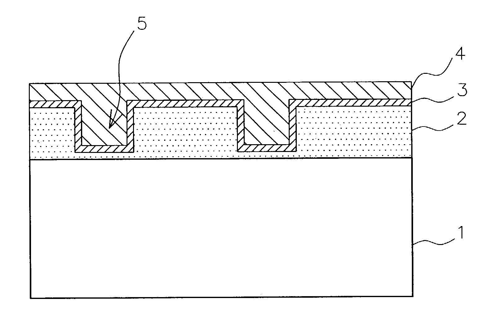
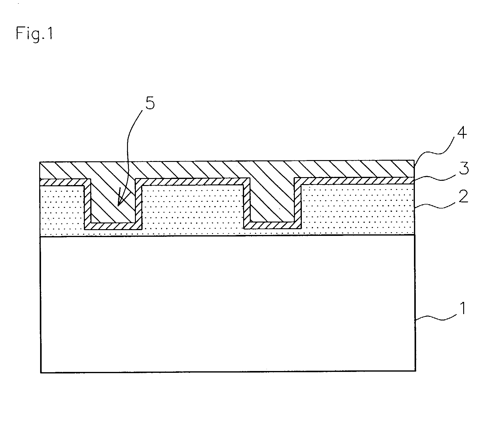
Process for chemical mechanical polishing of semiconductor substrate and aqueous dispersion for chemical mechanical polishing
a technology of chemical mechanical polishing and semiconductor substrate, which is applied in the direction of other chemical processes, lapping machines, manufacturing tools, etc., can solve the problems of reducing the removal rate of scratches, reducing the mechanical strength of layers, and suppressing the occurrence of scratches. , to achieve the effect of reducing the occurrence of scratches, and excellent removal ra
- Summary
- Abstract
- Description
- Claims
- Application Information
AI Technical Summary
Benefits of technology
Problems solved by technology
Method used
Image

Examples
examples 1 to 13
3. Examples 1 to 13 and Comparative Examples 1 to 6
[0147]Polishing performances of a copper film and an insulating layer were evaluated by using the aqueous dispersions [1] to [12] prepared as described above.
[0148]3-1. Evaluation of Polishing Performance of a Copper Film
[0149]An 8-inch thermal oxide film-coated silicon wafer on which copper film is formed (thickness of copper film; 15,000 Å, manufactured by Asahi Sangyo Co., Ltd.) was attached to a chemical mechanical polishing apparatus “EPO112” (trade name) manufactured by Ebara Corp. The surface of the copper film was polished with a polishing pad “IC1000” (trade name) manufactured by Rodel Nitta for 1 minute while supplying each of aqueous dispersion shown in Tables 1 to 3 at a rate of 300 ml / min under a pressing pressure and a rotation speed of a polishing table described in Tables 4 to 6. Maximal driving currents at the polishing table are shown in Tables 4 to 6.
[0150]In addition, a thickness of a copper film after polishing ...
PUM
| Property | Measurement | Unit |
|---|---|---|
| pressure | aaaaa | aaaaa |
| secondary particle diameter | aaaaa | aaaaa |
| secondary particle diameter | aaaaa | aaaaa |
Abstract
Description
Claims
Application Information