Radiation imaging device and system

a radiation imaging and imaging device technology, applied in radiation measurement, instruments, electrical equipment, etc., can solve the problems of limiting the planar area of the detector and readout substrate that can be bonded together, the imaging area is limited by current semiconductor manufacturing, and the imaging area is even more limited, so as to reduce or minimize the amount of imaging dead area, improve image quality, and increase the imaging area

Inactive Publication Date: 2007-03-13
OY AJAT LTD
View PDF19 Cites 35 Cited by
  • Summary
  • Abstract
  • Description
  • Claims
  • Application Information

AI Technical Summary

Benefits of technology

[0031]The architecture of the present invention utilizing an intermediate substrate as a mounting platform for the semiconductor substrates accomplishes several benefits desirable in a radiation imaging device. One of the benefits is the potential for producing larger area imaging devices with improved image quality relative to some prior devices by reducing or minimizing the amount of imaging dead area in the device. This is accomplished by having an entire ASIC readout substrate, including its I / O contacts, disposed within the “perimeter shadow” of its associated detector substrate. In this configuration, the ASIC readout substrate has no perimeter edge extending beyond the perimeter shadow of the detector substrate. Therefore, unitary detector substrates may be close packed using tiling techniques to form a mosaic imaging device that has minimized imaging dead area, because the underlying unitary readout substrates themselves do not have an imaging dead area.
[0032]Another potential benefit is the facilitation of production of radiation energy imaging devices that utilize semiconductor substrates which are sensitive to the temperatures and pressures of certain prior semiconductor radiation imaging device manufacture methods and technologies. For example, in situations where the semiconductor substrate is brittle, or is comprised of temperature sensitive materials, such detector substrates comprises Cadmium and / or Tellurium. This is particularly the case where solder bump-bonding is to be used to bond the conductive contacts of the semiconductor substrates. By initially applying the solder bumps to the conductive contacts on the intermediate substrate, the semiconductor substrates are not exposed to the sometimes harsher conditions required to initially make bumped contacts. The intermediate substrate is not a semiconductor substrate, and may be made of relatively more rugged materials as selectable by one of skill in the art to withstand the initial bumping conditions. Once the conductive contacts on a face of the intermediate substrate are bumped, conductive bonding to the corresponding conductive contacts of a sensitive semiconductor substrate may be accomplished using the potentially less harsh conditions of solder reflow techniques.

Problems solved by technology

However, the above noted SBBASIC imaging devices are unitary devices with an imaging area that is limited by current semiconductor manufacturing and bump-bonding technologies.
Imaging area is even more limited with the CMOS technology typically used to create the semiconductor readout substrates.
Even if semiconductor substrate dimensions are increased, current bump-bonding technology would still limit the planar area of the detector and readout substrates that can be bonded together (e.g., a 10 cm×10 cm monolithic detector substrate to its readout substrate).
However, tiling techniques have also introduced an amount of imaging dead area into the imaging area of the mosaic imaging device, which can adversely affect device's image quality.
Even though the depth of the wire bonding area is typically a few mm, it can create an imaging dead area that is unacceptably large for a particular radiation imaging application.
This is mechanically difficult in the production of imaging devices like the Lemercier device.
The wire bonding area is not sensitive to radiation and does not perform imaging.
This technique is complicated in its execution because the wedge-platform requires careful control of the tilt angle and precise alignment of the tile devices relative to each other.
Further more, the inactive area is never completely covered and the tile angle can introduce a parallax error depending on the angle of incidence of the incoming radiation.
While the SBBASIC technology is relatively the newest approach to direct radiation digital imaging and has advantages over the other prior radiation digital imaging technologies, it also currently has certain limitations:a. In current devices, the detector and readout substrates are manufactured with a limited field of view.
This is insufficient for most commercial applications.b. Due to this limitation, tiling techniques that combine a plurality of SBBASIC devices have been suggested to provide a larger field of view.
However, such tiling techniques can be cumbersome and difficult to implement on an industrial production scale.
This can adversely impact the quality of imaging and the cost of the complete camera head comprising a plurality of such SBBASICs.c. In addition to the limitation of (a) and (b) above, in current SBBASIC imaging devices, the interconnection of the ASIC with wire bonding pads introduces an “inactive” area for each SBBASIC device.
Such “dead” areas adversely impact image quality, especially when they are too large to cancel them out by software.

Method used


Image

  • Radiation imaging device and system
  • Radiation imaging device and system
  • Radiation imaging device and system

Examples


Embodiment Construction

[0051]Referring now to the drawings, the details of preferred embodiments of the present invention are graphically and schematically illustrated. Like elements in the drawings are represented by like numbers, and any similar elements are represented by like numbers with a different lower case letter suffix.

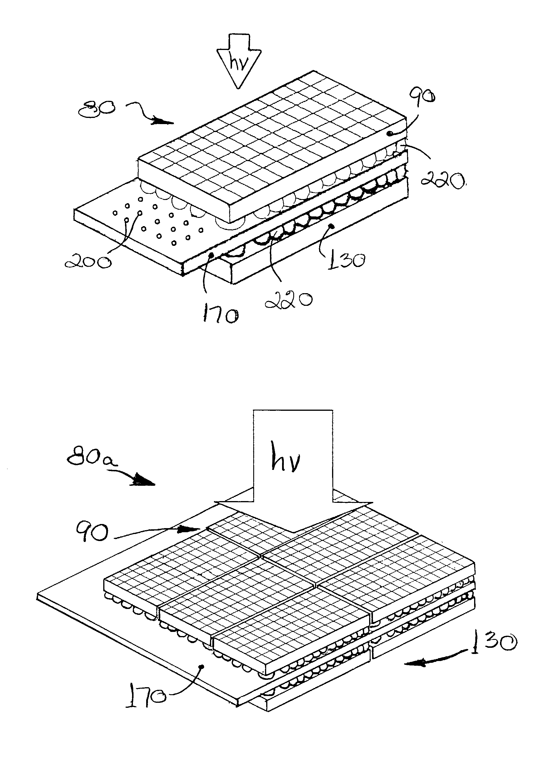
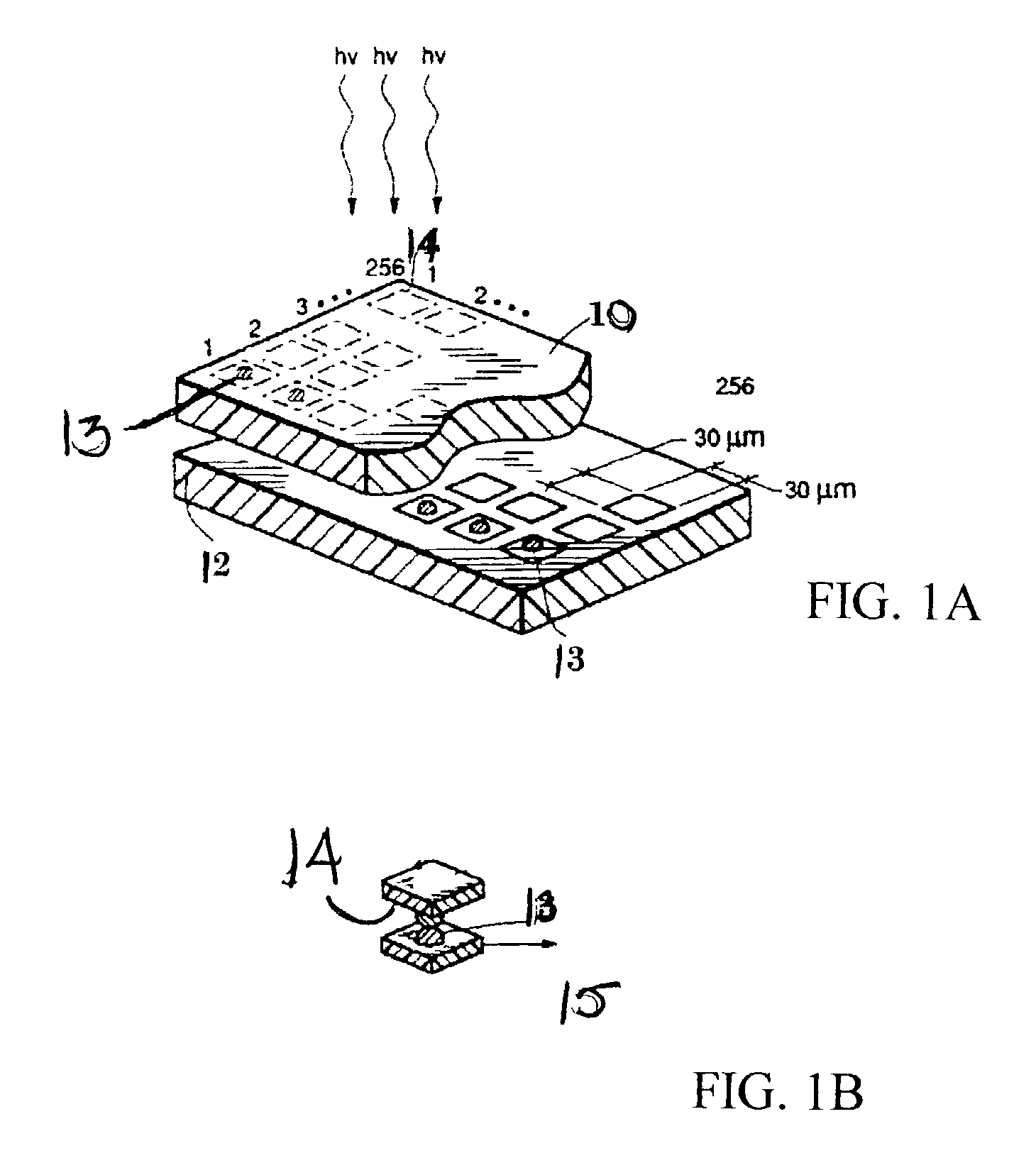
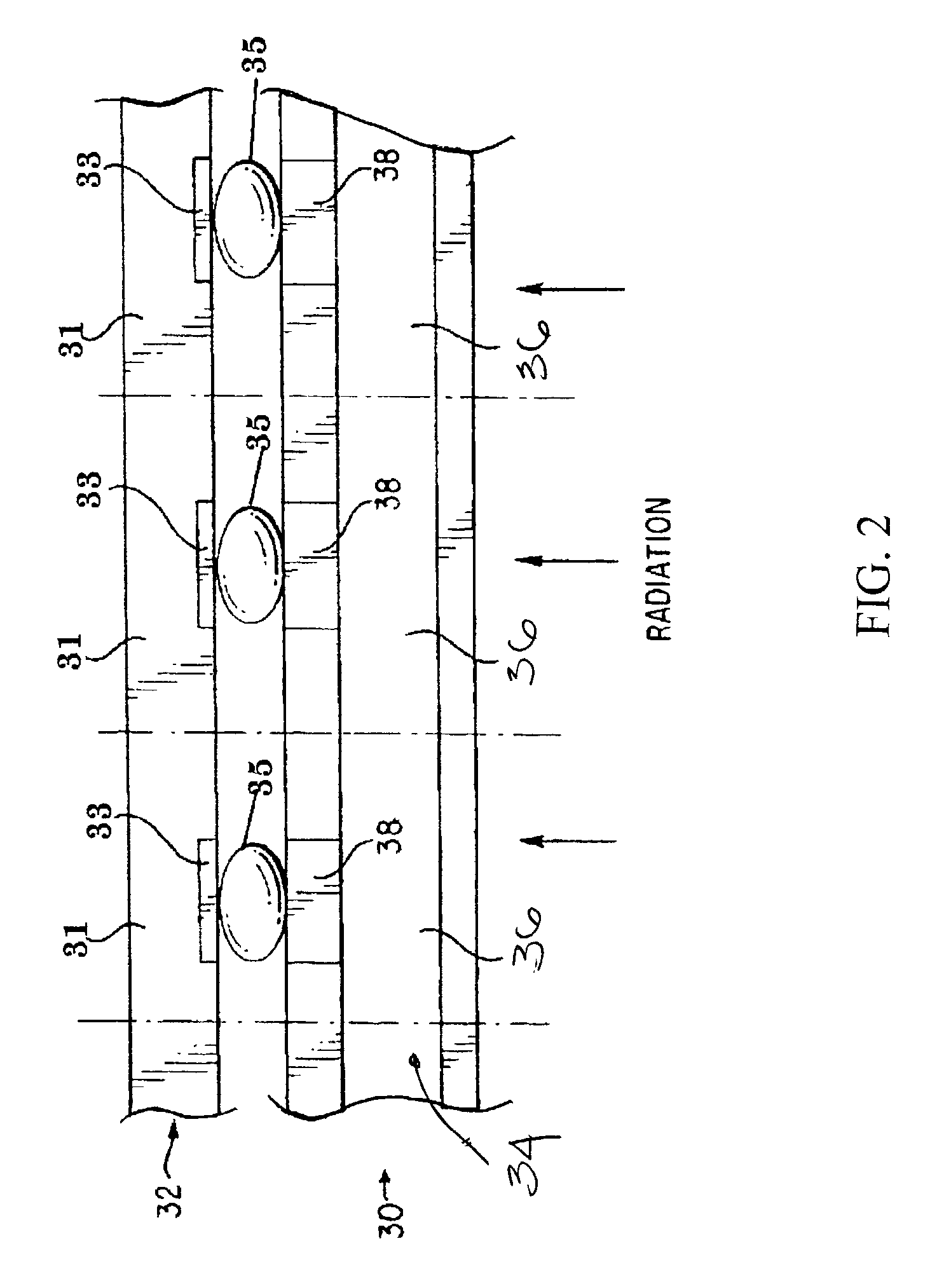
[0052]As exemplified in FIG. 5A, in a preferred embodiment, the present invention is a SVCASIC type digital imaging device 80 for imaging x-ray and gamma-ray radiation energy preferably in the energy range of 1 keV to 500 keV. The digital SVCASIC imaging device 80 comprises two semiconductor substrates, a detector substrate 90 and a readout / signal processing substrate 130, separated by and bonded to an intermediate substrate 170. The substrates 90, 130&170 have a substantially planar configuration and are disposed adjacent each other with their planes in a parallel to form a laminate structure in the assembled imaging device 80. In an alternative preferred embodiment exemplified i...


PUM


Abstract

An x-ray and gamma-ray radiation energy imaging device has its semiconductor detector substrate and semiconductor readout/processing substrate both mounted on opposite sides of, and electrically communicating through, an intermediate substrate. The substrates are all substantially planar with the top plan perimeter of the semiconductor readout/processing substrate falling within the top plan shadow perimeter of the corresponding semiconductor detector substrate with which it electrically communicates. Additionally, all of the readout/processing circuitry contacts of the semiconductor readout/processing substrate are disposed on the surface of the semiconductor readout/processing substrate that electrically communicates with the intermediate substrate. Substantially all electrical communication to and from the semiconductor readout/processing substrate is routed through the intermediate substrate. The intermediate substrate is a printed circuit board or similar construct. The electrical contacts between the semiconductor substrates and the intermediate substrate are accomplished using bump-bonds, conductive adhesive bonds, conductive adhesive films or a combination thereof. One or two dimensional planar arrays of semiconductor readout/processing substrates and corresponding semiconductor detector substrates can be mounted on a single intermediate substrate using “tiling” techniques known in the art to form a mosaic radiation imaging device of increased active imaging area and reduced/minimized imaging dead area.

Description

[0001]The present application claims the benefit of prior U.S. Provisional Application Ser. No. 60 / 364,248, filed 13 Mar. 2002, to which the present application is a regular U.S. National Application, and of prior filed Finland Application serial number 2002 0311, filed 15 Feb. 2002.FIELD OF THE INVENTION[0002]The present invention is in the field of semiconductor devices for detecting and image analyzing x-ray and gamma ray radiant energy above 1 keV. More specifically, the present invention relates to such devices wherein image analysis occurs by way of incident radiant energy on the device producing current flow between two electrically accessible points on two different semiconductor substrates separated by an intermediate substrate.BACKGROUND OF THE INVENTION[0003]Over the past ten years digital radiation imaging has gradually been replacing conventional radiation imaging where the recording means is film or an analog device such as an Image Intensifier. Currently, several such...

Claims


Application Information

Patent Timeline
Patent Type & Authority Patents(United States)
IPC IPC(8): G01T1/24G01T1/29H01L27/146
CPCG01T1/2928H01L27/14658H01L27/14661
Inventor SPARTIOTIS, KONSTANTINOSPUHAKKA, KIMMO PETTERI
Owner OY AJAT LTD
Why Eureka
Try Eureka