Semiconductor memory

a technology of semiconductors and memory, applied in the field of semiconductor memory, can solve the problems of generating reading out failure, mis-latching data, and increasing the difficulty of fuses, and achieve the effect of improving the resistance of factors and improving reliability

Active Publication Date: 2007-03-20
PANASONIC SEMICON SOLUTIONS CO LTD
View PDF4 Cites 7 Cited by
  • Summary
  • Abstract
  • Description
  • Claims
  • Application Information

AI Technical Summary

Benefits of technology

[0019]Main objects of the present invention therefore are to achieve improvements in the resistance for factors which deteriorates the properties, e.g., Vt dispersions of the MOS transistors to be mounted and the disturbance noises, and to achieve improvements in the reliability.
[0025]With the present invention, for example, it is possible to amplify the voltage by the voltage comparing circuit while keeping the voltage difference in accordance with the resistance difference. Thereby, it enables to perform a stable reading-out action which is highly resistant to dispersions in Vt (threshold voltage) of the MOS transistors of the voltage comparing circuit and to the noise at the time of reading out.
[0026]Furthermore, by controlling the semiconductor memory used for reading-out through a control signal which is formed with a one-shot pulse according to a reading-out-action command signal, consumption of electric current at the time of reading out can be reduced. In addition, it is possible to relieve stresses upon the electric fuse. With this, the reliability is further improved.
[0027]Moreover, by controlling the latch circuit and the voltage comparing circuit through a control signal formed with a pulse, it becomes possible to pre-charge the gates of the PMOS transistors which constitute the cross couple in the voltage comparing circuit, after data is latched by the latch circuit. Therefore, it enables to suppress the deterioration in the property of the PMOS transistor, which is caused due to a high bias applied between the gate and the substrate.
[0028]Furthermore, it becomes possible to start the voltage comparing circuit while keeping the voltage difference in accordance with the resistance difference. Therefore, it enables to dramatically improve the resistance to the dispersions in Vt of the MOS transistors which constitutes the voltage comparing circuit and to the noise at the time of reading out.
[0029]As described above, with the present invention, it is possible to perform a stable reading-out action, which is highly resistant to the dispersions in Vt of the MOS transistors and to the noise at the time of reading out.

Problems solved by technology

Fabrication of the fuses has become increasingly difficult due to its micronized process so that there has been a demand for developing a substitute technique.
That is, during the process of comparing and amplifying the small difference between the voltages, which is caused when the cross couple nodes N3, N4 are discharged from VDDH, there may cause mis-latching of data thus generating reading out failure.
Therefore, in such a system LSI which uses a plurality of semiconductor memories with a memory redundant function, consumption of electric current is increased.
Therefore, “0” is always applied to the gate of either the PMOS transistor 105 or 106 so that there may be a risk of deteriorating the PMOS transistor.

Method used


Image

  • Semiconductor memory
  • Semiconductor memory
  • Semiconductor memory

Examples


first embodiment

(First Embodiment)

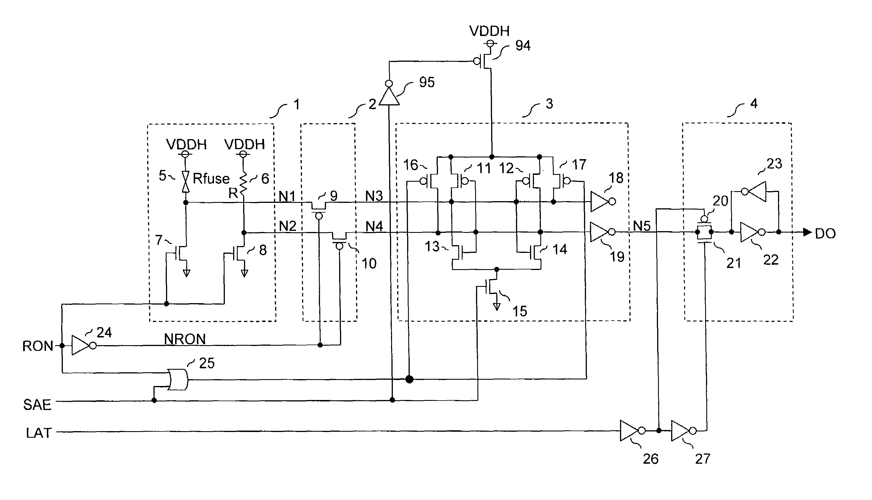
[0044]FIG. 1 shows an example of a semiconductor memory which comprises an electric fuse. In FIG. 1, reference numeral 1 is a voltage converting circuit. 2 is a switch circuit. 3 is a voltage comparing circuit. 4 is a latch circuit. RON is a control signal formed with a one-shot pulse, which controls the voltage converting circuit 1, the switch circuit 2, and the voltage comparing circuit 3. SAE is a control signal formed with a one-shot pulse, which controls the voltage comparing circuit 3. LAT is a control signal formed with a one-shot pulse, which controls the latch circuit 4.

[0045]The voltage converting circuit 1 comprises an electric fuse (a first resistance element) 5, a reference resistance (a second resistance element) 6, and NMOS transistors (NMOS switches) 7, 8. One end each of both the electric fuse 5 and the reference resistance 6 is connected to a power source VDD and the other end thereof is connected to GND (ground potential) through the NMOS transis...

second embodiment

(Second Embodiment)

[0086]In the case where the latch gate of the first embodiment (FIG. 1) is constituted of a MOS transistor with a thin gate oxide film, the voltage level of the control signal becomes as follows. That is, the control signals RON, SAE have the voltage level which is boosted from the VDD to the VDDH according to the external input signal NFR (VDD level), whereas the control signal LAT becomes the voltage level of the VDD. However, under such voltage properties, if the voltage converting circuit 1 and the voltage comparing circuit 3 are controlled by the control signal RON, SAE of the VDDH level and the latch circuit 4 is controlled by the control signal LAT of the VDD level, there may cause a following inconvenience. Specifically, when the VDD is the low voltage and the VDDH is the high voltage, there may be a timing skew generated between the control signals RON, SAE of the VDDH level and the control signal LAT of the VDD level. Such timing skew will be described b...

third embodiment

(Third Embodiment)

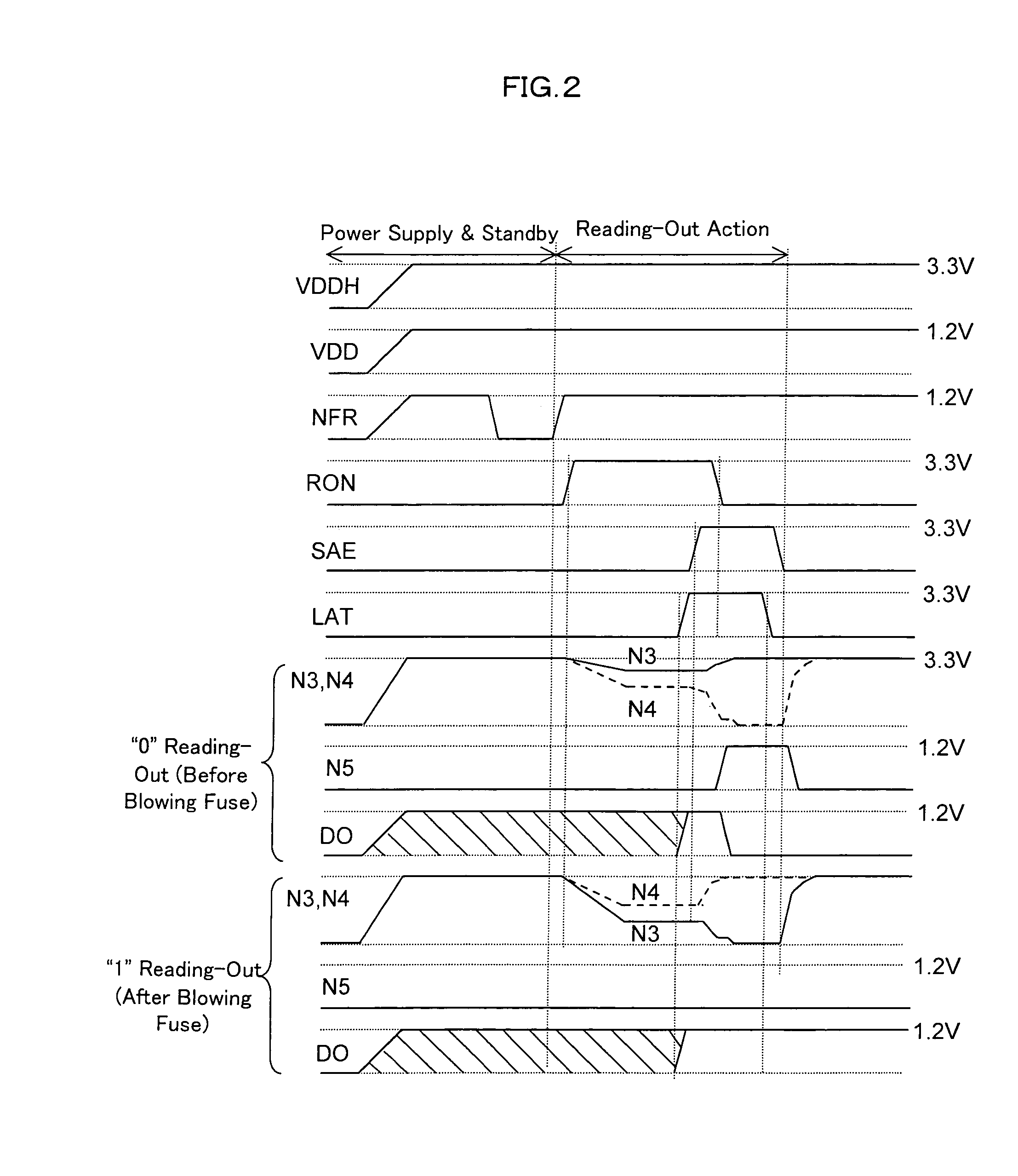
[0089]There may be manufacture dispersions and blown-resistance dispersions generated in the initial resistance of the electric fuse 5 or the resistance value thereof after the blowout even if the electric fuse 5 is formed by using any selected types of materials. For example, in the semiconductor memory comprising the electric fuse 5, if the resistance value of the electric fuse 5 is the value with a smaller margin with respect to the reference resistance 6, the resistance value fluctuates when the electric fuse 5 is energized while being used as a product. Thus, a reading-out failure may be caused. Such failures happen even if, during the inspection, the “0” reading-out action and “1” reading-out action are normally carried out for the value of the reference resistance 6.

[0090]In order to avoid such failures in advance, the semiconductor memory of this embodiment comprises a circuit structure which checks the resistance value margins before and after the blowout ...


PUM


Abstract

Provided is a semiconductor memory, comprising: a voltage converting circuit which voltage-converts a resistance difference between a first and a second resistance elements; a voltage comparing circuit which outputs an output corresponding to the voltage conversion; a latch circuit for holding the output of the voltage comparing circuit; and a switch circuit which cuts and connects the voltage converting circuit and the voltage comparing circuit.

Description

BACKGROUND OF THE INVENTION[0001]1. Field of the Invention[0002]The present invention relates to a semiconductor memory and, more particularly, to a semiconductor memory comprising a resistant element such as a silicide blown electric fuse which can be manufactured through a standard CMOS process.[0003]2. Description of the Related Art[0004]In a semiconductor memory with analog trimming or memory redundancy, fuse elements are widely used for achieving the functions. Fabrication of the fuses has become increasingly difficult due to its micronized process so that there has been a demand for developing a substitute technique. For meeting such demand, there is proposed an electric fuse which can be easily manufactured by a standard CMOS process to be used for storing data by using a difference of the resistance before and after blowing silicide.[0005]The related art is disclosed, for example, in U.S. Pat. No. 6,384,664 “DIFFERENTIAL VOLTAGE SENSE CIRCUIT TO DETECT THE STATE OF A CMOS PR...

Claims


Application Information

Patent Timeline
Patent Type & Authority Patents(United States)
IPC IPC(8): G11C7/00
CPCG11C7/065G11C17/18G11C7/14
Inventor KAWASAKI, TOSHIAKIAGATA, MASASHISHIRAHAMA, MASANORINISHIHARA, RYUJI
Owner PANASONIC SEMICON SOLUTIONS CO LTD
Why Eureka
Try Eureka