Method and apparatus for clock-and-data recovery using a secondary delay-locked loop

a delay-locked loop and clockanddata technology, applied in the field of clockanddata recovery systems, can solve the problems of limiting the noise filtering of the data channel, increasing the bit error rate, and challenging the design of low-jitter phase-locked loops, so as to achieve optimal allocation of loop bandwidth for each function, avoid jitter peaking, and wide bandwidth

Active Publication Date: 2007-03-27
GLOBALFOUNDRIES US INC
View PDF13 Cites 12 Cited by
  • Summary
  • Abstract
  • Description
  • Claims
  • Application Information

AI Technical Summary

Benefits of technology

[0011]An object of the present invention is to prevent perturbing the clock by unwanted channel noise.
[0016]With the unique and unobvious aspects of the present invention, a two-part topology performs clock-and-data recovery operations in two steps. The topology employs a delay-locked loop to make the data retiming process independent of a clock signal recovery function, in which the clock signal is extracted from the data channel by a phase-locked loop. The phase-locked loop extracts the clock information from a noisy serial stream of non-return-to-zero data and tracks the long-term jitter, while a delay-locked loop having a wide loop bandwidth performs data synchronization in the phase domain and tracks the short-term jitter. The separation of these functions allows the designer to optimally allocate the loop bandwidth for each function.
[0017]With the present invention, one can provide a narrow or moderate bandwidth for the phase-locked loop for a clean clock signal and can provide a wide bandwidth for the delay-locked loop for prompt jitter tracking without creating jitter peaking. With the present invention, the jitter peaking can be avoided with wide loop bandwidth since the delay-locked loop (first order loop) does not create overshoot in a jitter transfer function. The present invention offers wider loop bandwidth than typical phase-locked loop clock-and-data recovery systems.
[0019]The present invention also provides a solution for parallel link data communications based on clock signal recovery from a single channel, which avoids the use of multiple voltage-controlled oscillators.

Problems solved by technology

In clock-and-data recovery systems, noise is an overriding design concern.
Thus, to design a low-jitter phase-locked loop is challenging in many ways due to stringent jitter budgets and loop bandwidth specifications.
However, wide loop bandwidth can limit the noise-filtering from the data channel as the noise bandwidth increases.
As the clock is perturbed by unwanted channel noise, the bit-error rate will increase simply due to the clock itself Therefore, there is a fundamental tradeoff in choosing loop bandwidth between the clock extraction and the data retiming.

Method used


Image

  • Method and apparatus for clock-and-data recovery using a secondary delay-locked loop
  • Method and apparatus for clock-and-data recovery using a secondary delay-locked loop
  • Method and apparatus for clock-and-data recovery using a secondary delay-locked loop

Examples


second exemplary embodiment

[0035

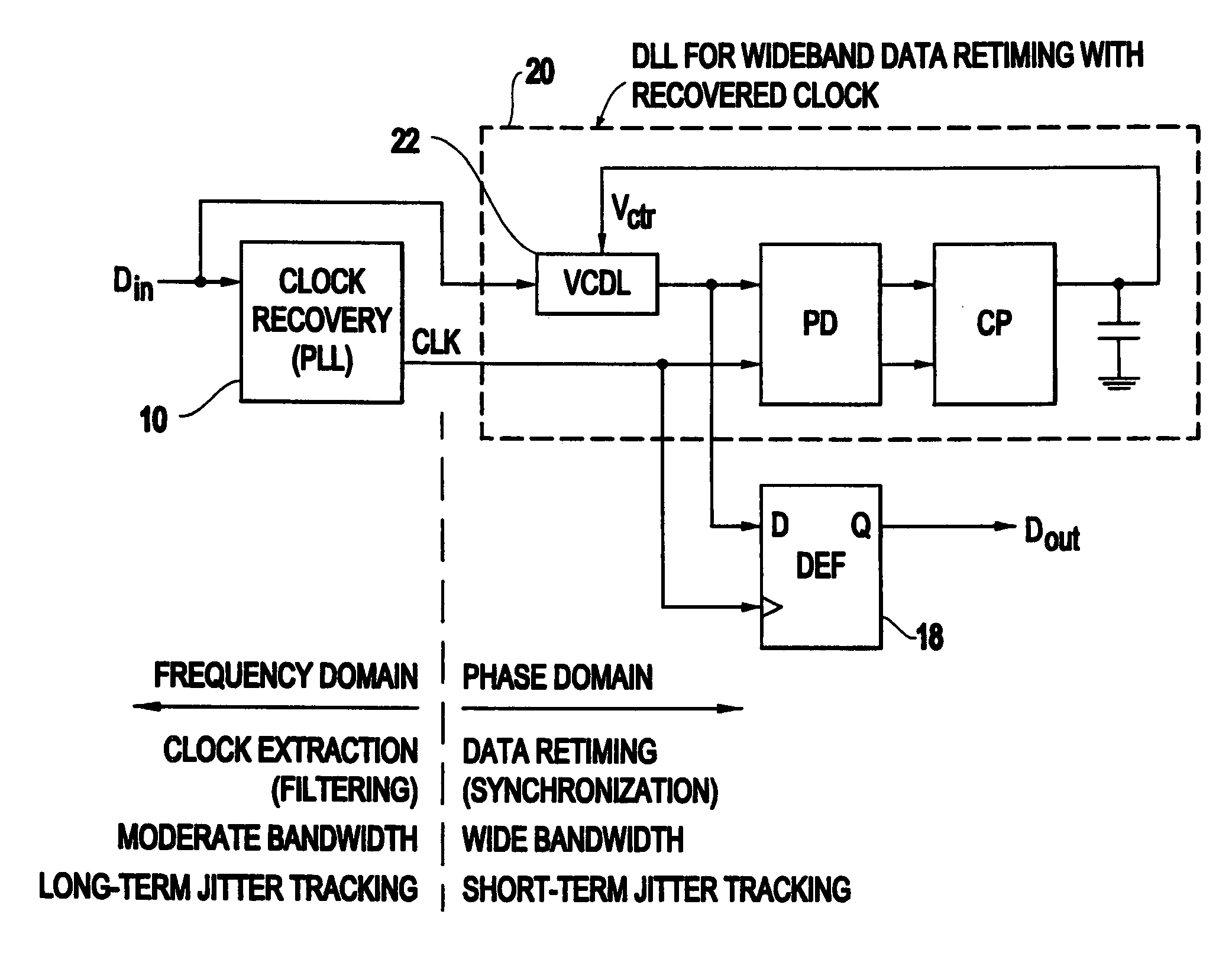
[0036]When only data synchronization is required without jitter transfer consideration, an alternative way to implement the delay-locked loop 20 in accordance with a second exemplary embodiment of a clock-and-data recovery circuit of the present invention is to delay the clock instead of the data, as shown in FIG. 4. This embodiment offers simpler implementation since delaying the clock does not demand group-delay consideration in voltage-controlled delay line design.

third exemplary embodiment

[0037

[0038]FIG. 5 shows a block diagram of a third exemplary embodiment of the clock-and-data recovery system in accordance with the present invention for half-rate demultiplexers. When a divide-by-2 circuit is necessary for the half-rate demultiplexers 32, the delay-locked loop 30 with a half-rate phase detector 34 can also perform delay compensation for the divide-by-2 circuit 36. In FIG. 5. an in-phase signal (I) and a quadrature phase signal (Q) are generated from the divide-by-2 circuit 36 to support half-rate phase detection. Since both rising and falling edges of the clock signal are aligned to the data in the half-rate demultiplexer scheme, a quadrature phase (Q) is needed to sample the data as shown in FIG. 5.

[0039]The present invention also offers data-pattern-independent bang-bang phase detection when binary phase detectors are used. A conventional bang-bang phase detector (BBPD) generates an error voltage to control the voltage-controlled oscillator, resulting in frequen...

fourth exemplary embodiment

[0040

[0041]A fourth exemplary embodiment of a clock-and-data recovery circuit in accordance with the present invention, shown in FIG. 7 which provides parallel link data communications without using multiple voltage-controlled oscillators.

[0042]As shown in FIG. 7, one phase-locked loop 40 provides the clock recovery, and four delay-locked loops 42, 44, 46 and 48, perform data retiming for four different data channels. Compared to having four clock-and-data recovery circuits, the topology shown in FIG. 7 requires only a single voltage-controlled oscillator instead of four voltage-controlled oscillators as would be demanded by a four-clock-and-data recovery circuit approach. Reducing the number of on-chip voltage-controlled oscillators is particularly beneficial because voltage-controlled oscillators are very sensitive to noise coupling and crosstalk, which may result in consuming more area for isolation.

[0043]Compared to methods using a phase rotator, the present invention does not e...


PUM


Abstract

A clock and data recovery circuit includes a delay-locked-loop adapted to recover data from a data stream: and a phase-locked-loop in communication with the delay-locked-loop and adapted to recover a clock signal from the data stream.

Description

BACKGROUND OF THE INVENTION[0001]1. Field of the Invention[0002]The present invention generally relates to clock-and-data recovery systems where a periodic clock signal is to be extracted from non-periodic data, and the same clock is then used to sample data with a minimum of errors.[0003]2. Description of the Related Art[0004]Phase-locked loop circuits play a critical role in high speed data communications. They are used in clock-and-data recovery circuits, in which clock and data are recovered from a single high-speed serial stream of non-return-to-zero data. Ethernet, Fibre Channel, and SONET / SDH transmission systems are specific examples of systems that typically use phase-locked loop-based clock-and-data recovery circuits.[0005]FIG. 1 shows a block diagram of a conventional phase-locked loop-based clock-and-data recovery 10, which has a phase detector 12, a loop filter 14, and a voltage-controlled oscillator 16. The phase-locked loop-based clock-and-data recovers circuit 10 is ...

Claims


Application Information

Patent Timeline
Patent Type & Authority Patents(United States)
IPC IPC(8): H03D3/24H04L7/00H03L7/07H03L7/081H04L7/033
CPCH03L7/07H03L7/0812H04L7/0037H04L7/033H04L7/0041
Inventor RHEE, WOOGEUNFRIEDMAN, DANIELGOWDA, SUDHIRSOYUER, MEHMET
Owner GLOBALFOUNDRIES US INC
Why Eureka
Try Eureka