Optical wiring substrate fabrication process and optical wiring substrate device

Active Publication Date: 2007-03-27
ADTEC ENG +1
View PDF14 Cites 11 Cited by
  • Summary
  • Abstract
  • Description
  • Claims
  • Application Information

AI Technical Summary

Benefits of technology

[0012]In light of the circumstances described above, an object of the present invention is to provide a fabrication method capable of simple formation by maskless exposure of optical wiring circuitry, particularly of inclined face forms for providing reflection mirrors at end portions of optical waveguides, and / or capable of simple formation by maskless exposure of circuit structures in which optical wiring circuitry is formed at a plurality of levels in a lamination direction, and to provide an optical wiring substrate provided with such optical wiring circuitry.

Problems solved by technology

However, in the example of JP-A No. 6-265738 mentioned above, because the photo mask has a particular structure, fabrication thereof is troublesome.
Furthermore, in the technique of JP-A No. 2002-82242, two photolithography processes are required for working of mirror formation portions, and the production process is more complicated.
In such cases, with substrate materials such as polyimide and the like for which moisture absorption is high and dimensional variations are large, positional accuracy of the mirror formation portions are adversely affected by expansion and contraction of the material.
As a result, there are problems in that production processes are complicated and production costs rise.
Therefore, when a multi-layered circuit is to be formed as described above, high accuracy positioning and mirror formation are subject to the same issues.

Method used


Image

  • Optical wiring substrate fabrication process and optical wiring substrate device
  • Optical wiring substrate fabrication process and optical wiring substrate device
  • Optical wiring substrate fabrication process and optical wiring substrate device

Examples


first embodiment

Structure of Exposure Apparatus

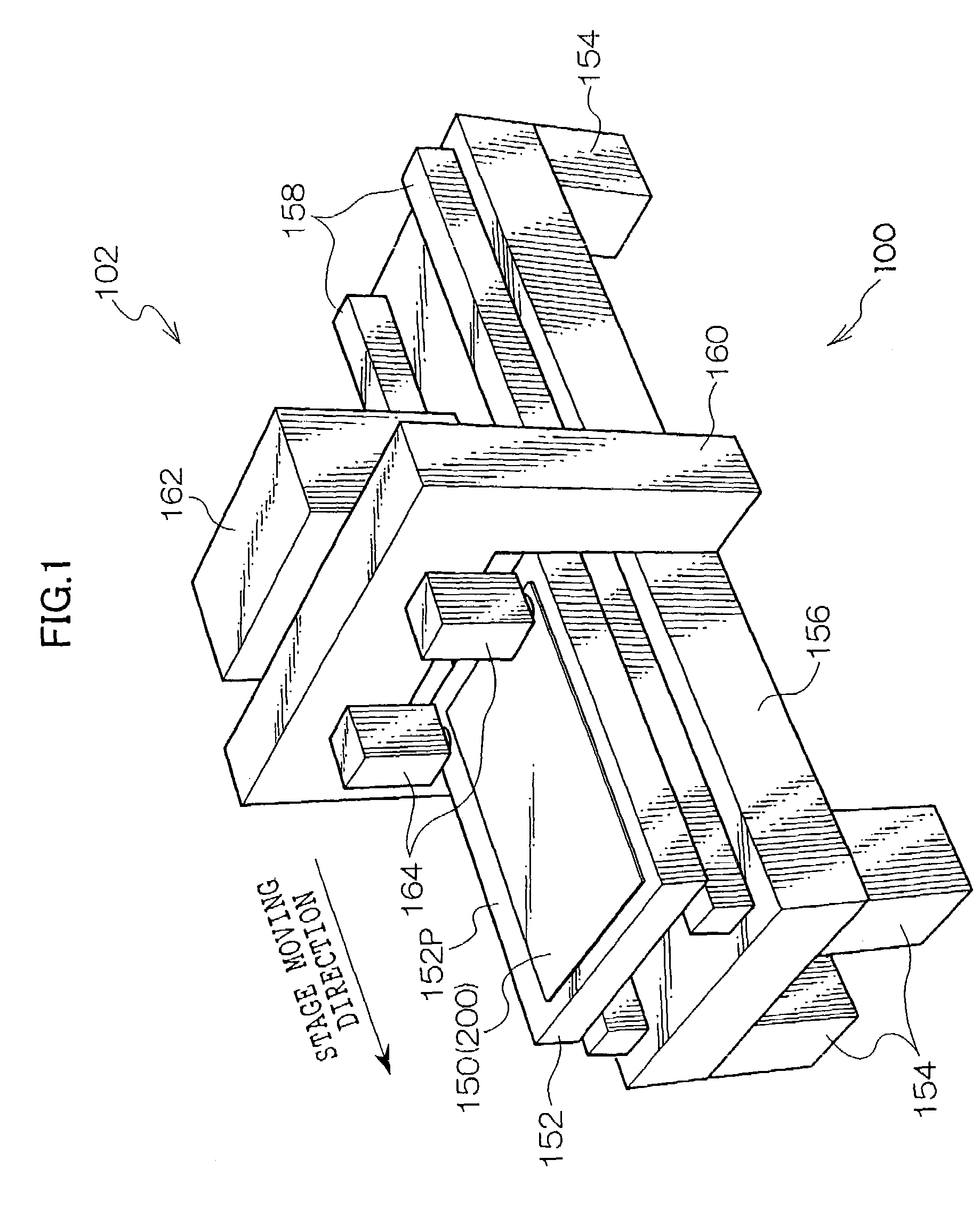
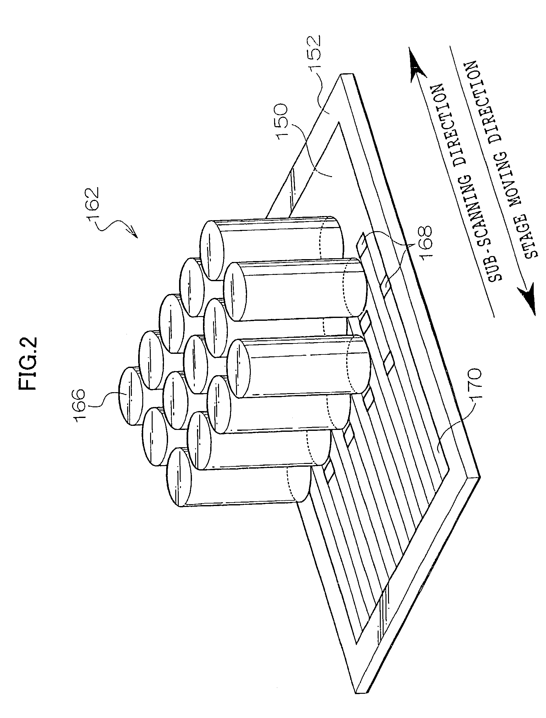
[0096]As shown in FIG. 1, an exposure apparatus 100 relating to a first embodiment of the present invention is provided with a flat board-form stage 152, which adsorbs and retains an optical wiring substrate (optical wiring substrate material) 200 at a surface thereof. At the optical wiring substrate 200, a sheet-form photosensitive material (a photoresist) 150 is layer-formed on an optical waveguide material. Two guides 158, which extend in a stage movement direction (the direction of arrow in the drawing), are provided at an upper face of a thick board-form equipment pedestal 156, which is supported at four leg portions 154. The stage 152 is disposed such that a longitudinal direction thereof is oriented in the stage movement direction, and is supported by the guides 158 so as to be reciprocatingly movable. In this exposure apparatus 100, an unillustrated driving apparatus is provided for driving the stage 152 along the guides 158.

[0097]At a central ...

second embodiment

[0163]Next, a method of fabricating an optical wiring substrate in which an optical wiring circuit is provided with a plurality of levels will be described.

[0164]FIGS. 20 and 21 show an exposure apparatus for forming an optical wiring circuit with a plurality of levels, which relates to a second embodiment of the present invention. In this exposure apparatus 171, a stage 172 is formed with a transparent glass plate of a predetermined thickness (for example, 10 mm). Pairs of rails 176 are provided respectively above and below the stage 172. The rails 176 are disposed to be parallel along a longitudinal direction of the stage 172 (the upper side rails 176 are not shown in the drawings). At each pair of rails 176, a line-form scanner 162A or 162B, which is provided with a plurality of the aforementioned exposure heads 166, is provided traversing a width direction of the stage 172 (the main scanning direction). The scanners 162A and 162B are controlled and driven by an unillustrated dri...

third embodiment

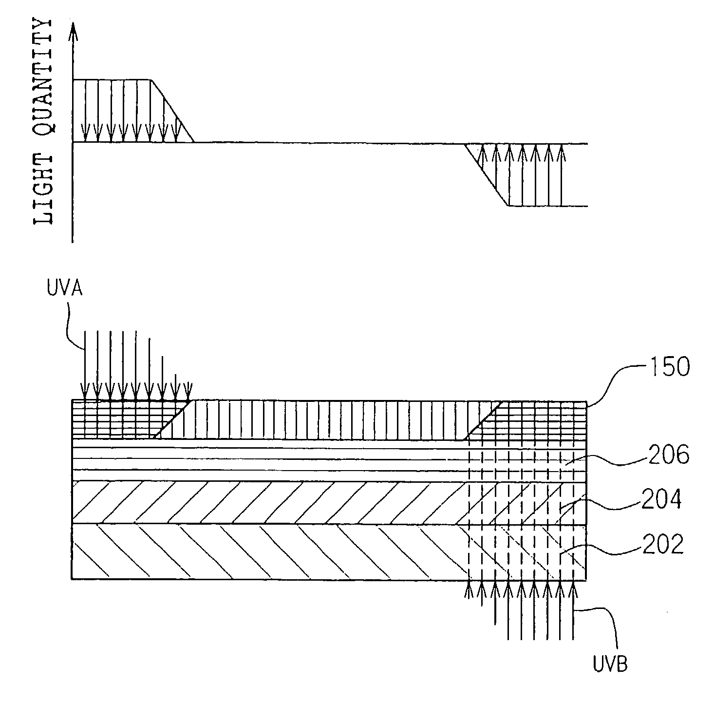
[0180]Next, a method for fabricating an optical wiring substrate (optical wiring circuitry) using the exposure apparatus 100 described for the first embodiment, by using a photo-bleaching method, will be described.

[0181]FIGS. 25A to 25F show a process for fabricating an optical wiring substrate by a photo-bleaching method. First, in FIG. 25A, a cladding layer 222 is formed by coating and baking polyvinylidene fluoride (PVDF) at the temporary support 202. In FIG. 25B, a core layer 224 is formed on the cladding layer 222 by coating and baking polysilane, which serves as a polymer material for photo-bleaching, and which has a refractive index larger than that of the cladding layer 222 and has a characteristic of being sensitive to UV light such that the molecular structure thereof changes and the refractive index falls.

[0182]This optical wiring substrate material is set on the stage 152 of the exposure apparatus 100 and a predetermined exposure pattern is exposed at the core layer 224 ...


PUM


Abstract

An optical wiring substrate fabrication method capable of simple formation, by maskless exposure, of an inclined face shape at an end portion of a core layer structuring an optical waveguide. Using an exposure apparatus, image exposure is carried out with a light beam which is modulated by a spatial modulation element in accordance with image information. A predetermined area of a photosensitive material (a photoresist), which is coated on the core layer which is a material of the optical wiring substrate, is exposed by a light beam (UV) and patterned to form an etching mask. A region corresponding to the inclined face, which is to be formed at the end portion of the core layer, is exposed and patterned by the light beam, exposure amounts of which are controlled in accordance with the inclined form of the inclined face, such that an end portion of the etching mask has an inclined face structure. When the core layer is worked by etching using this etching mask, working of the core layer at the end portion of the core layer progresses in proportion to film thickness of the etching mask, and the inclined face is formed.

Description

BACKGROUND OF THE INVENTION[0001]1. Field of the Invention[0002]The present invention relates to a fabrication process and device of an optical wiring substrate.[0003]2. Description of the Related Art[0004]At an optical wiring substrate which is provided with optical wiring circuitry, which is structured as a circuit by optical waveguides (for example, an optical wiring circuit in which light is transmitted and the like by surface mounted-type light-emitting elements and light-receiving elements), light paths are changed by 90° between light paths at the surface mounted-type elements and light paths in the optical waveguides of the optical wiring substrate. Thus, the light is fed into the optical waveguides and emitted from the optical waveguides. End portions of the optical waveguides may accordingly be formed at an inclination of 45°, with reflection mirrors being provided at these inclined end faces.[0005]Conventionally, in order to form an inclined surface at an end portion of a...

Claims


Application Information

Patent Timeline
IPC IPC(8): G02B6/12G02B6/136G02B6/138G03F7/20
CPCG02B6/136G02B6/138G03F7/70391G03F7/7005G03F7/70291G02B2006/12104
Inventor NAKAYA, DAISUKEFUJII, TAKESHIOKAZAKI, YOJINAGANO, KAZUHIKOISHIKAWA, HIROMI
Owner ADTEC ENG
Why Eureka
Try Eureka