Process for passivating polysilicon and process for fabricating polysilicon thin film transistor

a technology of polysilicon and thin film transistor, which is applied in the direction of transistors, semiconductor devices, electrical devices, etc., can solve the problems of reducing the hydrogenation efficiency, reducing the passivation efficiency, and generally not being able to undergo a process on the device, so as to shorten the passivation time and increase the passivation efficiency

Active Publication Date: 2007-04-03
INNOLUX CORP
View PDF5 Cites 7 Cited by
  • Summary
  • Abstract
  • Description
  • Claims
  • Application Information

AI Technical Summary

Benefits of technology

[0006]An object of the present invention is to solve the above-mentioned problems and provide a process for passivating polysilicon, which increases the passivation efficiency and shortens the passivation time.

Problems solved by technology

Hydrogen atoms, however, diffuse out at high temperature, rendering the previous hydrogenation ineffective.
Therefore, after hydrogenation, the device generally cannot be subjected to a process with higher temperature (such as 450° C.).
However, at this time, there are several layers of coating on the polysilicon thin film channel, which greatly reduces the hydrogenation efficiency.
In addition, the bonding between hydrogen and silicon atoms is very weak, and easily broken during device operation.
Therefore, using hydrogen atoms to fill in defects frequently reduces device reliability.

Method used


Image

  • Process for passivating polysilicon and process for fabricating polysilicon thin film transistor
  • Process for passivating polysilicon and process for fabricating polysilicon thin film transistor
  • Process for passivating polysilicon and process for fabricating polysilicon thin film transistor

Examples


Embodiment Construction

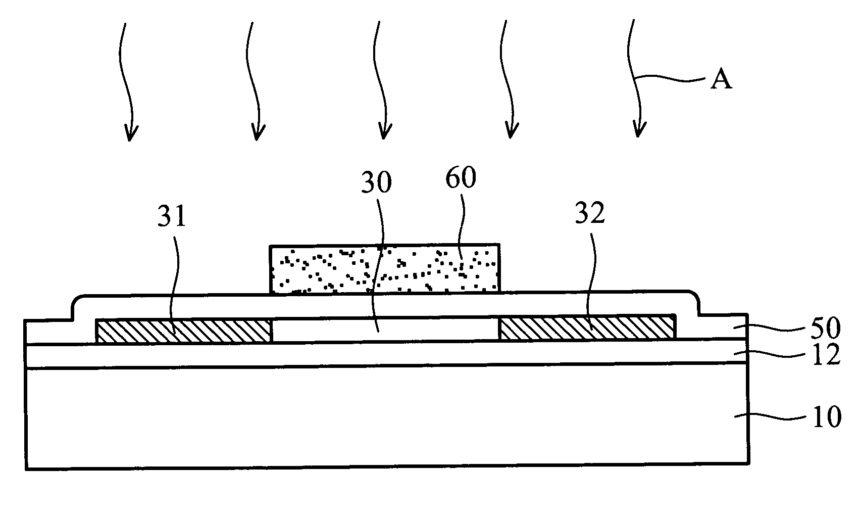
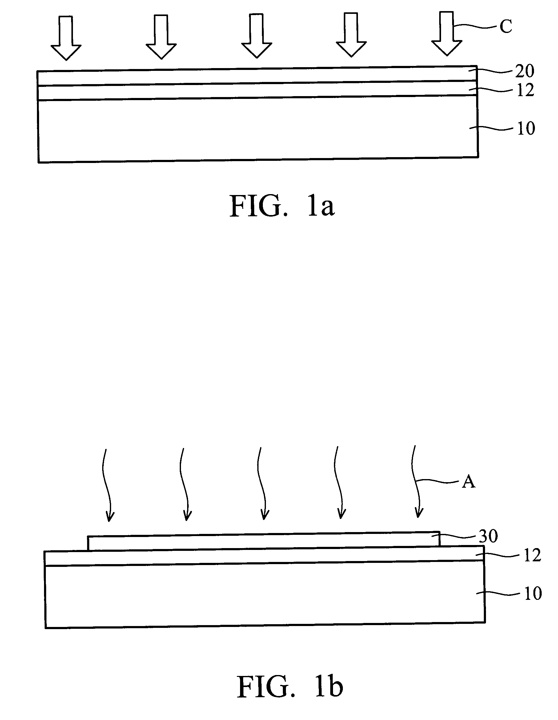
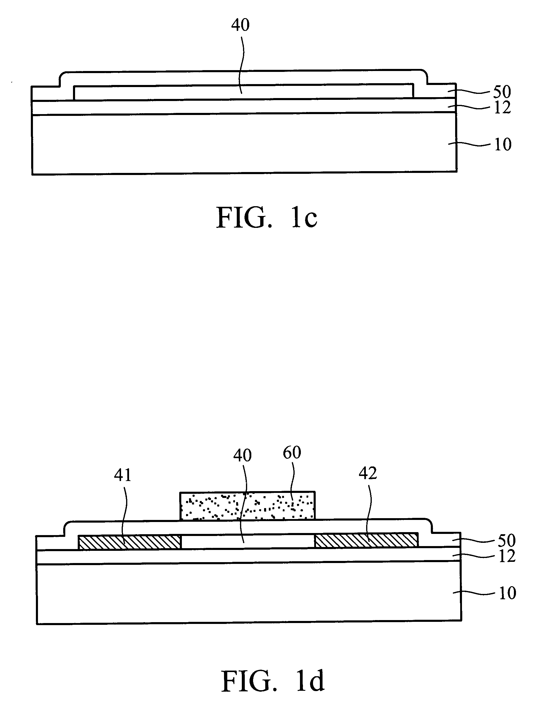
[0016]The feature of the present invention resides in that the atom used is able to form a stronger bond with a silicon atom, such as F, N, or O, to fill in the polysilicon defect. Specifically, high pressure annealing is performed using a fluorine-containing gas, a chlorine-containing gas, an oxygen-containing gas, a nitrogen-containing gas, or mixtures thereof to passivate the polysilicon layer. Thus, a polysilicon thin film transistor with better electric properties and reliability can be obtained. The timing and / or sequence of passivating the polysilicon layer is not limited. Passivation can be performed directly after the polysilicon layer is formed without forming other films. Or, passivation can be performed after the polysilicon layer and the gate dielectric layer are formed. Or, passivation can be performed after the polysilicon layer, the gate dielectric layer, and the gate are formed. Or, passivation can be performed after the polysilicon layer, the gate dielectric layer,...


PUM

PropertyMeasurementUnit
pressureaaaaaaaaaa
pressureaaaaaaaaaa
temperatureaaaaaaaaaa

Abstract

A process for passivating polysilicon and a process for fabricating a polysilicon thin film transistor. A polysilicon layer is formed. Next, high-pressure annealing is performed using a fluorine-containing gas, a chlorine-containing gas, an oxygen-containing gas, a nitrogen-containing gas, or mixtures thereof to passivate the polysilicon layer.

Description

BACKGROUND OF THE INVENTION[0001]1. Field of the Invention[0002]The present invention relates to a process for passivating polysilicon, and more particularly to a process for passivating polysilicon by means of high pressure annealing using a fluorine-containing gas, a chlorine-containing gas, an oxygen-containing gas, a nitrogen-containing gas, or mixtures thereof for fabrication of polysilicon thin film transistors.[0003]2. Description of the Prior Art[0004]In polysilicon thin film transistors (p-Si TFTs), the grain boundary of polysilicon or the defect density in the grains plays an important role in the electric properties of TFTs. Reducing the defect density can greatly enhance the electric properties of the TFTs. One method of reducing the defect density is to increase the polysilicon grain size and crystallinity. Another method is to introduce other atomic components into polysilicon to fill in the defects, this process is generally referred to as passivation.[0005]Due to sma...

Claims


Application Information

Patent Timeline
Patent Type & Authority Patents(United States)
IPC IPC(8): H01L21/302H01L21/461H01L21/314H01L21/316H01L21/318H01L21/324H01L21/336H01L29/786
CPCH01L21/314H01L21/31662H01L21/3185H01L29/78675H01L29/66757H01L29/78603H01L21/324H01L21/02107H01L21/02238H01L21/0217
Inventor LIN, CHING-WEI
Owner INNOLUX CORP
Why Eureka
Try Eureka