Architecture and methods for computing with reconfigurable resistor crossbars

a technology of resistor crossbars and architecture, applied in the field of electronic devices, can solve the problems of high implementation cost, inability to scale well, and the miniaturization that has accompanied the growth of si ics

Active Publication Date: 2007-04-10
HEWLETT-PACKARD ENTERPRISE DEV LP
View PDF14 Cites 33 Cited by
  • Summary
  • Abstract
  • Description
  • Claims
  • Application Information

AI Technical Summary

Problems solved by technology

However, because of a combination of physical and economic reasons, the miniaturization that has accompanied the growth of Si ICs is reaching its limit.
The major problem with (1) is that the wafer on which the devices are built must be aligned to within a small fraction of the size of the device features in at least two dimensions for several successive stages of lithography, followed by etching or deposition to build the devices.
This level of control does not scale well as device sizes are reduced to nanometer scale dimensions.
It becomes extremely expensive to implement as devices are scaled down to nanometer scale dimensions.
The major problem with (2) is that it is a serial process, and direct writing a wafer full of complex devices, each containing trillions of components, could well require many years.
Finally, the problem with (3) is that high information content molecules are typically macromolecular structures such as proteins or DNA, and both have extremely complex and, to date, unpredictable secondary and tertiary structures that cause them to twist into helices, fold into sheets, and form other complex 3D structures that will have a significant and usually deleterious effect on their desired electrical properties as well as make interfacing them to the outside world impossible.

Method used


Image

  • Architecture and methods for computing with reconfigurable resistor crossbars
  • Architecture and methods for computing with reconfigurable resistor crossbars
  • Architecture and methods for computing with reconfigurable resistor crossbars

Examples


Embodiment Construction

Definitions

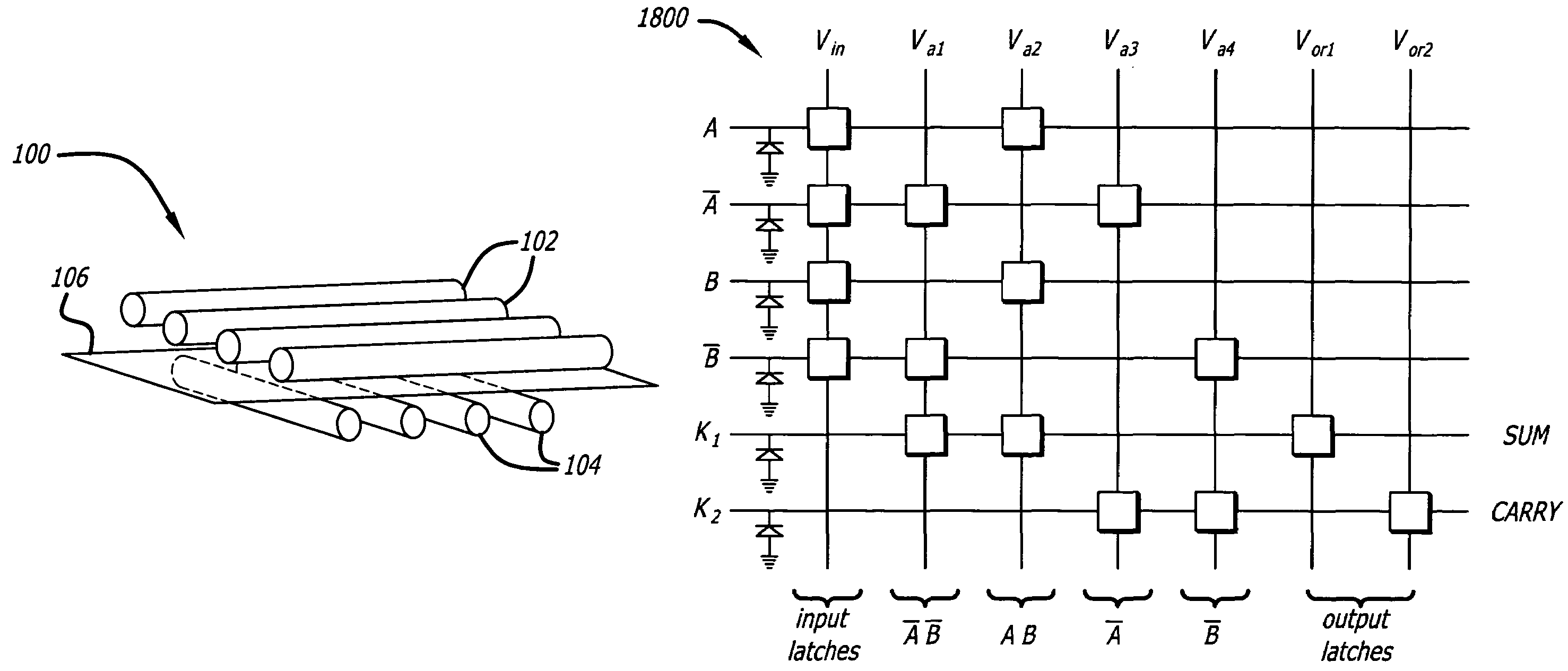
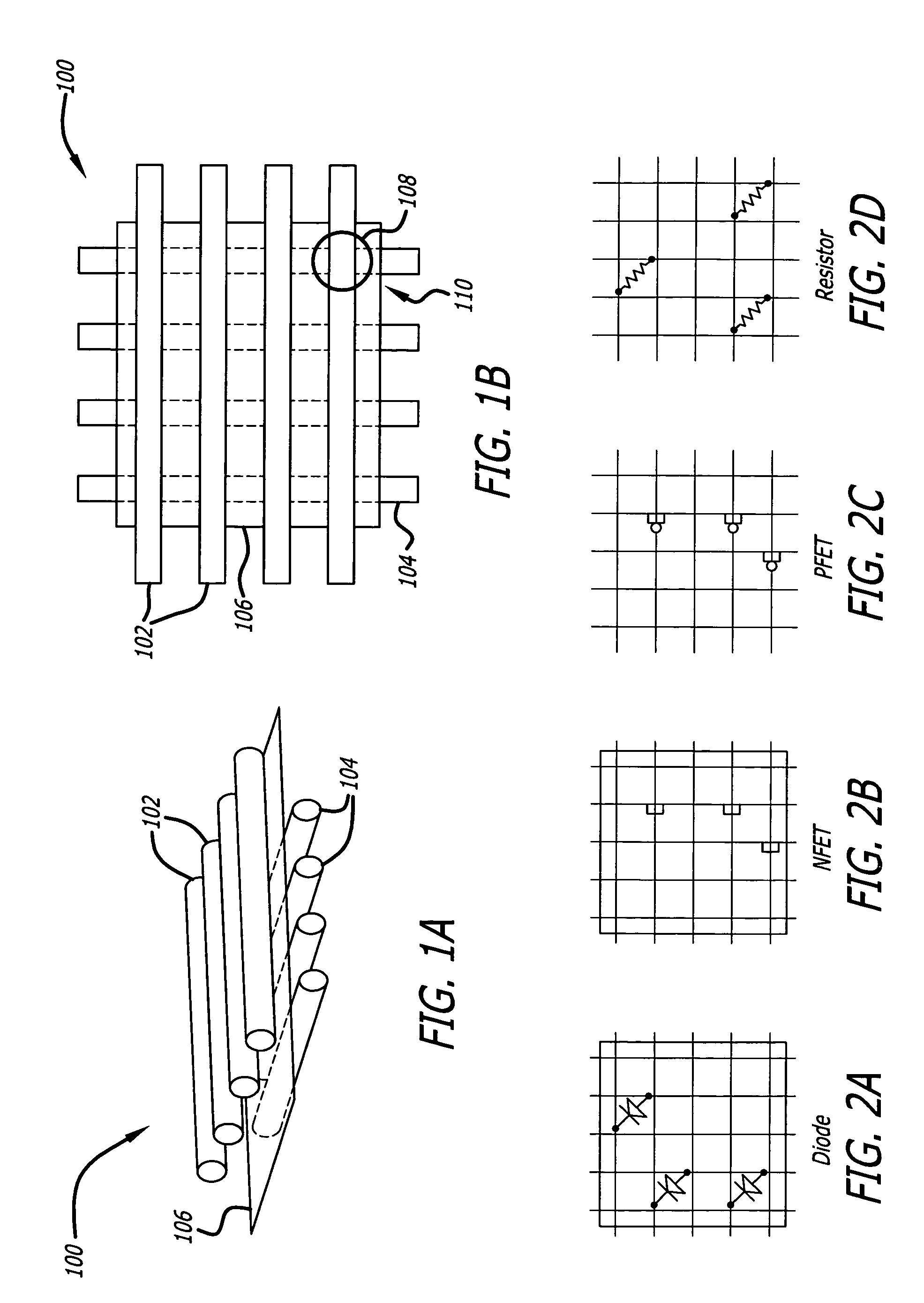
[0029]As used herein, the term “reconfigurable” means that a switch can change its state multiple times via a reversible process such as an oxidation or reduction; in other words, the switch can be opened and closed multiple times, such as the memory bits in a random access memory (RAM).

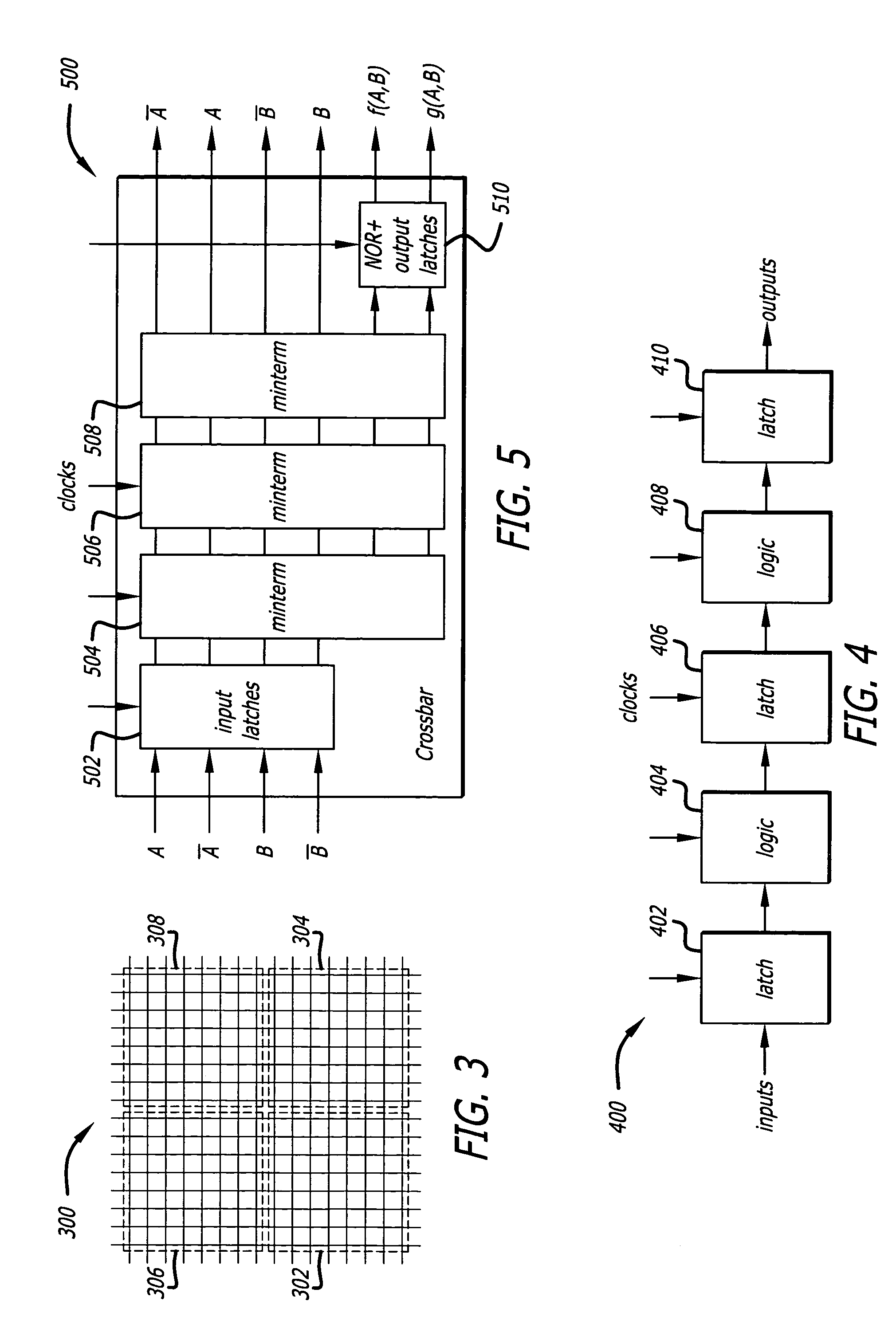
[0030]A “latch” is a digital electronic component capable of storing a single bit of information. It has an input line, an output line and one or more control lines. Generally the control lines manipulate the latch to be in one of two modes: in “programming mode,” the data on the input line is sampled and captured and stored in the memory element of the latch; in “output mode” (which may overlap “programming mode”) the stored data value is driven out, perhaps with an inversion, onto the output data line. Thus, a latch is a storage device that can sample and save a logic signal while also providing a mechanism for restoring the electrical integrity of that signal.

[0031]Micron-scale dimensio...


PUM


Abstract

An architecture for computing includes nanometer scale crossbar switches configured to perform a logical function in response to a sequence of pulses that encode logic values in the nanometer scale crossbar switches as impedances.

Description

TECHNICAL FIELD[0001]The present invention relates generally to electronic devices whose functional length scales are measured in nanometers, and, more particularly, to devices used as building blocks to form more complicated structures, and to methods for using such devices. Electronic devices both of micrometer and nanometer scale may be constructed in accordance with the teachings herein.BACKGROUND ART[0002]The silicon (Si) integrated circuit (IC) has dominated electronics and has helped it grow to become one of the world's largest and most critical industries over the past thirty-five years. However, because of a combination of physical and economic reasons, the miniaturization that has accompanied the growth of Si ICs is reaching its limit. The present scale of devices is on the order of tenths of micrometers. New solutions are being proposed to take electronics to ever smaller levels; such current solutions are directed to constructing nanometer-scale devices.[0003]Prior propo...

Claims


Application Information

Patent Timeline
Patent Type & Authority Patents(United States)
IPC IPC(8): G06F13/00H01L27/28H01L51/00H03K19/02H03K19/177
CPCB82Y10/00H03K19/02H01L27/285H01L51/0595Y10S977/708H10K19/202H10K10/701
Inventor SNIDER, GREGORY STUART
Owner HEWLETT-PACKARD ENTERPRISE DEV LP
Why Eureka
Try Eureka