Display device having a terminal that has a transparent film on top of a high resistance conductive film

a technology of conductive film and display device, which is applied in the direction of identification means, instruments, show hangers, etc., can solve the problems of increasing line resistance, and unable to provide the structure for suppressing the increase in contact resistance. , to achieve the effect of enhancing connection reliability

Active Publication Date: 2007-04-17
TRIVALE TECH
View PDF14 Cites 2 Cited by
  • Summary
  • Abstract
  • Description
  • Claims
  • Application Information

AI Technical Summary

Benefits of technology

[0009]In view of the foregoing, it is an object of the present invention to provide a secure electrical connection between the drive circuit and the terminals on the insulating substrate in the display device with the drive circuit mounted directly on an insulating substrate, thereby enhancing connection reliability.

Problems solved by technology

This increases line resistance and causes defects such as malfunction of the drive circuit.
Though the above conventional techniques provide the structures of display devices with a drive circuit mounted directly on the terminals of an insulating substrate, they do not provide the structure for suppressing the increase in contact resistance due to the material of the lines and terminals of the insulating substrate.
When mounting the drive circuit on the insulating substrate by the COG technique, it is difficult to form large line patterns of the power line and signal lines in the area where the drive circuit is mounted for resistance reduction, as described above.
Otherwise, it causes low voltage supply capacity or voltage drop in the power line, delay in the signal lines, and so on, which leads to malfunction of the drive circuit.
On the other hand, lines connected to the lines in a display area of the insulating substrate where pixels are to be formed do not necessarily have such a low resistance.

Method used


Image

  • Display device having a terminal that has a transparent film on top of a high resistance conductive film
  • Display device having a terminal that has a transparent film on top of a high resistance conductive film
  • Display device having a terminal that has a transparent film on top of a high resistance conductive film

Examples


embodiment 1

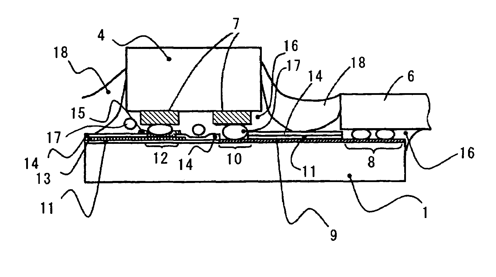
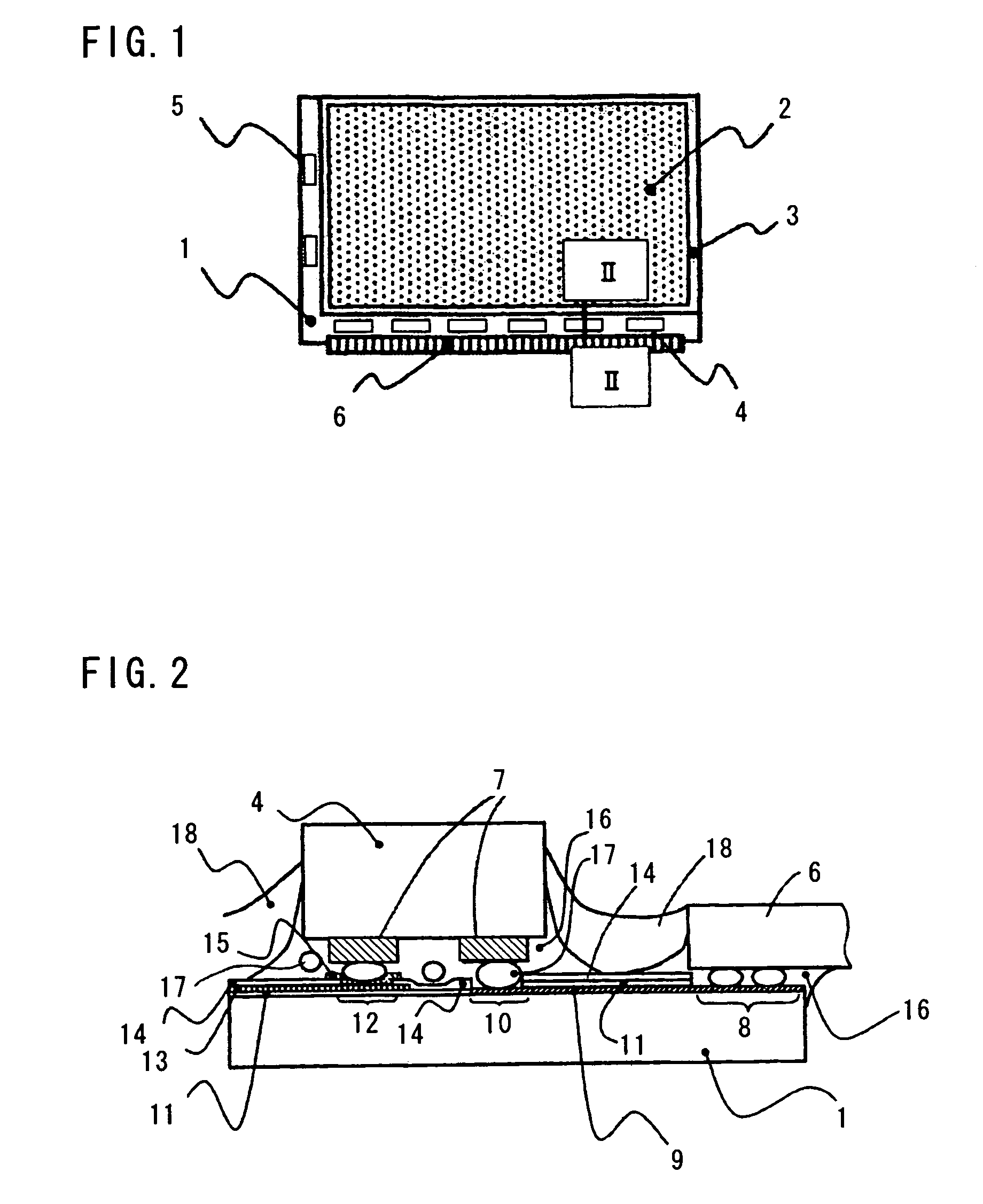
[0033]The first embodiment of the present invention will be explained hereinafter with reference to FIGS. 1 and 2. FIG. 1 is a plan view of a display device according to the first embodiment of this invention and FIG. 2 is a cross-sectional view along line II—II in FIG. 1. As shown in FIG. 1, the display device has an insulating substrate 1 having a display area 2 consisting of pixels. A color filter substrate 3, which serves as a counter substrate, is placed face to face with the insulating substrate 1 with liquid crystal interposed therebetween. On the peripheral area of the insulating substrate 1 outside of the display area are mounted a signal line drive circuit 4 comprising the lines to be connected to the pixels and connected to signal lines for supplying signals and a scan line drive circuit 5 comprising the lines connected to the pixels for driving the pixels. Further, a flexible substrate 6 is attached to the periphery of the insulating substrate 1 so as to supply power or ...

embodiment 2

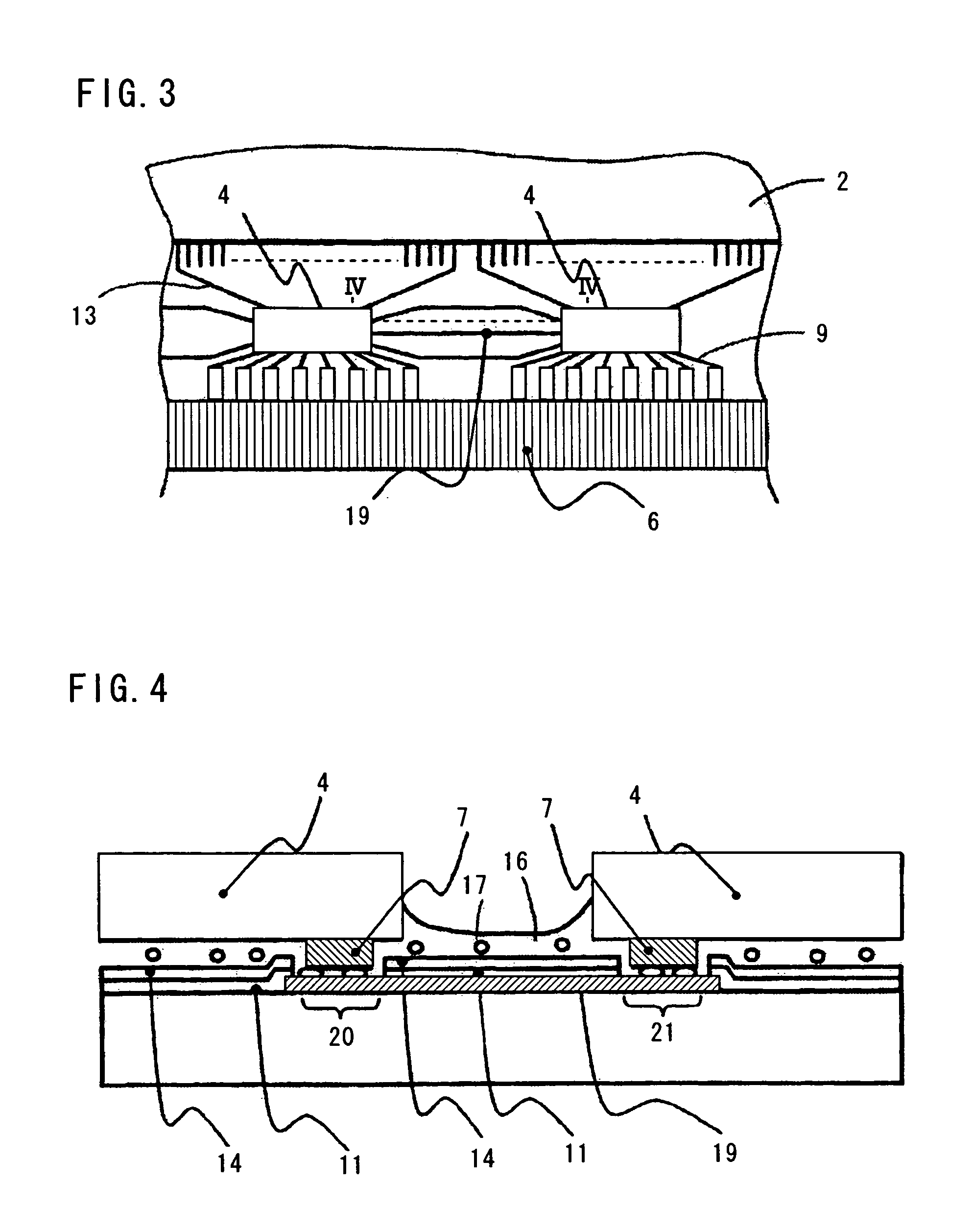
[0040]The second embodiment of the present invention will be explained herein after with reference to FIGS. 3 and 4. FIG. 3 is a plan view of a drive circuit mounting area of a display device according to the second embodiment of the present invention and FIG. 4 is a cross-sectional view along line IV—IV in FIG. 3. In FIGS. 3 and 4, the same elements as in FIGS. 1 and 2 are denoted by the same reference symbols, and the explanation will be given on the differences. FIGS. 3 and 4 illustrate the adjacent two drive circuits 4. The drive circuits 4 are connected by a drive circuit connecting line 19 connecting between the terminals formed at the sides of the two drive circuits 4 facing each other. If a signal is supplied from the signal line drive circuit 4 in the left to that in the right in FIG. 4, for example, the terminals 7 of the signal line drive circuit 4 are connected to the terminal 20 for supplying a signal and to the terminal 21 for receiving the signal, both formed on the i...

embodiment 3

[0042]The third embodiment of the present invention will be explained hereinafter with reference to FIGS. 5 and 6. FIG. 5 is a plan view of a drive circuit mounting area of a display device before a drive circuit is mounted, according to the third embodiment of this invention. FIG. 6 is a plan view of a drive circuit mounting area of another display device before a drive circuit is mounted, according to the third embodiment of this invention. In FIGS. 5 and 6, the same elements as in FIG. 1 to 4 are denoted by the same reference symbols, and the explanation will be given on the differences. FIG. 5 shows the terminals on the insulating substrate before the drive circuit is mounted. In this embodiment, the line terminals 12 to be connected to the lead lines 13 connected to the pixels of the display area 2 are formed in the drive circuit mounting area of the insulating substrate 1 along the side adjacent to the display area 2. Two lines of the line terminals 12 are formed in this examp...


PUM

PropertyMeasurementUnit
pressureaaaaaaaaaa
temperatureaaaaaaaaaa
thicknessaaaaaaaaaa

Abstract

The display device includes the lead line connected to pixels, the line terminal connected to the lead line and connected to the terminal of the drive circuit mounted directly on the insulating substrate by the conductive material through the transparent conductive film, the external terminal to be connected to an external unit, an external line connected to the external terminal, and an external line terminal connected to the external line and connected directly to the terminal of the drive circuit by the conductive material. The surface of the line terminal to be connected to the transparent conductive film is formed by the high resistance conductive film, and the surface of the external line terminal to be connected to the terminal of the drive circuit by the conductive material is formed by the low resistance conductive film.

Description

BACKGROUND OF THE INVENTION[0001]1. Field of the Invention[0002]The present invention relates to a display device with enhanced connection reliability between terminals on the insulating substrate and a drive circuit directly mounted thereon, and a method of manufacturing the display device, which are particularly effective in application to liquid crystal display devices.[0003]2. Description of the Related Art[0004]One advanced application that has been developed as a low-cost manufacturing method of display devices, such as liquid crystal display devices, is Chip-On-Grass (COG), in which a drive circuit is mounted directly on an insulating substrate. This technique directly attaches a drive circuit where Au bumps are created to terminals formed on the periphery of an insulating substrate with a conductive material such as an anisotropic conductive film (ACF). When using this technique, a power line and signal lines for driving the drive circuit are connected to the terminals (bump...

Claims


Application Information

Patent Timeline
Patent Type & Authority Patents(United States)
IPC IPC(8): G02F1/1345G02F1/13G09F9/00G09F9/30
CPCG02F1/13452A47F1/126A47F7/285A47F13/00
Inventor MORISHITA, HITOSHIUEDA, HIROSHIIWANAGA, HIROFUMINOUMI, SHIGEAKIYAMAGUCHI, TAKEHISA
Owner TRIVALE TECH
Why Eureka
Try Eureka