High frequency switch module and multi-layer substrate for high frequency switch module

a high-frequency switch module and multi-layer substrate technology, applied in waveguide type devices, transmission monitoring, modulation, etc., can solve the problems of complicated circuit, difficult design and fabrication of high-frequency switch prototypes, and longer period of time for reducing the dimensions of high-frequency switches using pin diodes, etc., to suppress the power of frequency components of harmonics, simple configuration, and easy design

Active Publication Date: 2007-04-17
SNAPTRACK
View PDF42 Cites 25 Cited by
  • Summary
  • Abstract
  • Description
  • Claims
  • Application Information

AI Technical Summary

Benefits of technology

[0011]It is an object of the invention to provide a high frequency switch module that has a simple configuration and that is easy to design and capable of suppressing the power of frequency components of harmonics, and to provide a multi-layer substrate used for the high frequency switch module.
[0014]According to the first high frequency switch module of the invention, the phase adjusting lines adjust the phase difference between the progressive wave of the harmonic and the reflected wave, so as to suppress the power of frequency components of the harmonics traveling from the high frequency switch toward the antenna port.
[0018]According to the second high frequency switch module of the invention, the phase adjusting lines adjust the phase difference between the progressive wave of the harmonic and the reflected wave, so as to suppress the power of frequency components of the harmonics traveling from the high frequency switch toward the antenna port.

Problems solved by technology

The high frequency switches using PIN diodes have a problem that the circuit is made more complicated as the number of frequency bands to switch increases, and it takes a longer period of time to design and fabricate prototypes of high frequency switches having required characteristics.
In particular, to make devices operable in the four bands of the EGSM, the American GSM (AGSM), the DCS and the PCS, or the five bands of the EGSM, the AGSM, the DCS, the PCS and the wideband code division multiple access (WCDMA), it is more difficult to design and reduce the dimensions of the high frequency switches using the PIN diodes.
Moreover, if the number of frequency bands to switch increases, the high frequency switches using the PIN diodes have a problem that harmonics produced by a nonconducting PIN diode increase and a problem that a current for making the PIN diodes conducting increases, which affects the period of time for which the cellular phone is operable for speech.
On the other hand, the high frequency switch using the GaAs-FET has a problem that, when a transmission signal of large power passes through the switch, the nonlinear characteristic of the GaAs-FET causes distortion of the transmission signal which then causes harmonics of a frequency of ‘n’ times the frequency of the transmission signal, where ‘n’ is an integer equal to or greater than 2.
Cellular phones having such high frequency switches are not acceptable.
Therefore, high frequency switches using GaAs-FETs are not popular among cellular phones for the GSM.
As a result, a small number of high frequency switches with GaAs-FETs are used, and the yield of phones satisfying the standard is poor, which prevents a reduction in price.
It is therefore impossible to reject the harmonics of the frequency of twice the frequency of a GSM transmission signal by using a filter in a dual-band cellular phone operable in the GSM and DCS.
However, according to the high frequency switch using the GaAs-FET, harmonic components increase if the operational voltage is reduced, so that it is difficult to provide the high frequency switches using GaAs-FETs with good yields.
It is therefore extremely difficult to satisfy the above-described characteristics only by improving the high frequency switches using the GaAs-FETs.

Method used


Image

  • High frequency switch module and multi-layer substrate for high frequency switch module
  • High frequency switch module and multi-layer substrate for high frequency switch module
  • High frequency switch module and multi-layer substrate for high frequency switch module

Examples


Embodiment Construction

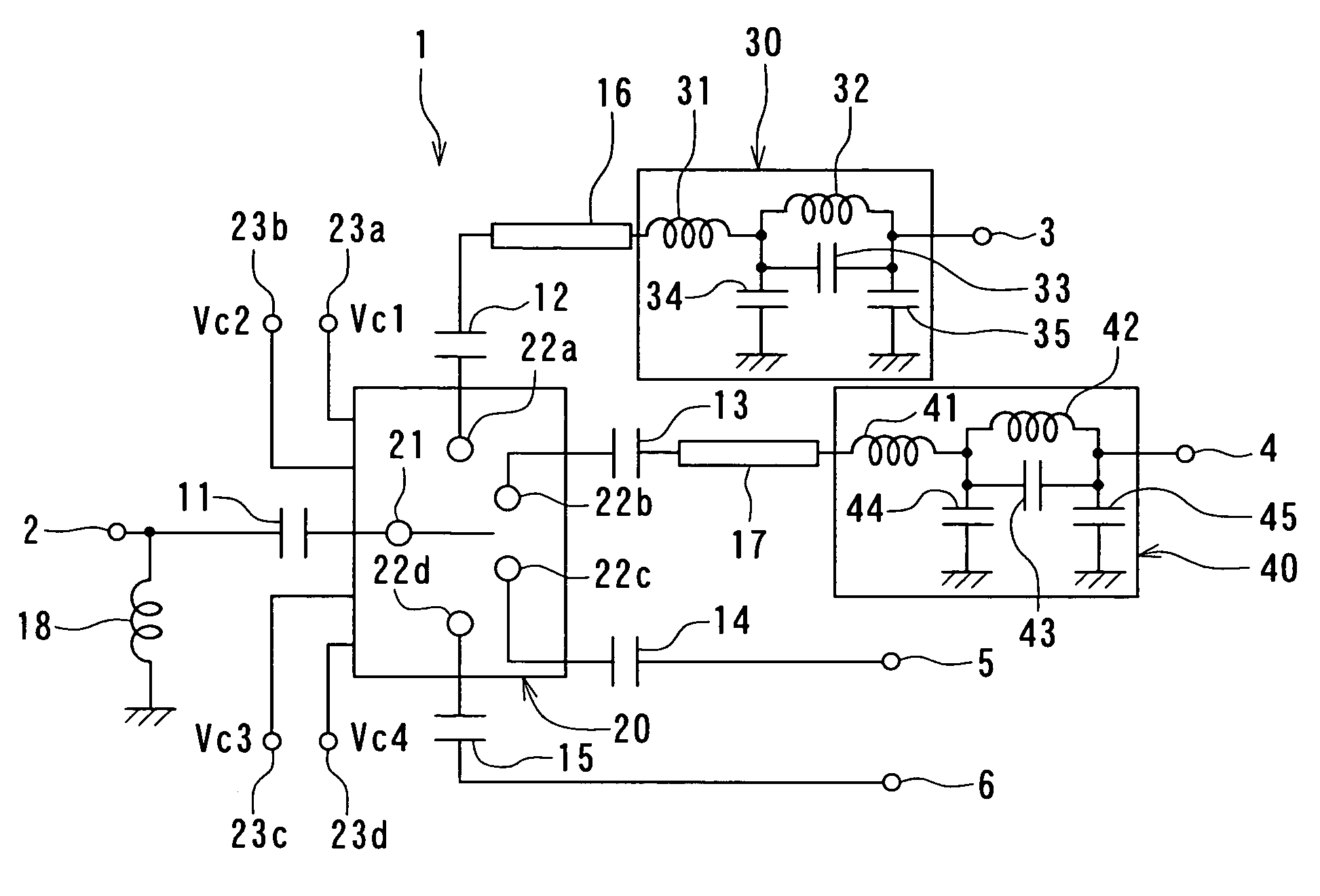
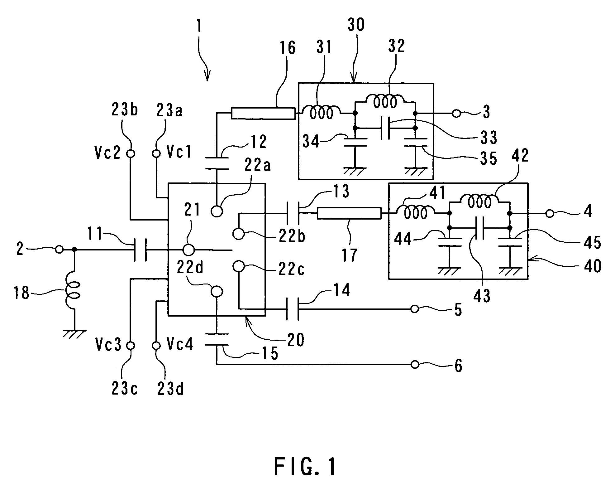
[0036]A preferred embodiment of the invention will now be described in detail with reference to the accompanying drawings. Reference is now made to FIG. 1 to describe an example of the circuit configuration of a high frequency switch module of the embodiment of the invention. In the embodiment the high frequency switch module 1 for processing GSM transmission signals and reception signals and processing DCS transmission signals and reception signals will be described by way of example.

[0037]The frequency band of GSM transmission signals is 880 to 915 MHz. The frequency band of GSM reception signals is 925 to 960 MHz. The frequency band of DCS transmission signals is 1710 to 1785 MHz. The frequency band of DCS reception signals is 1805 to 1880 MHz.

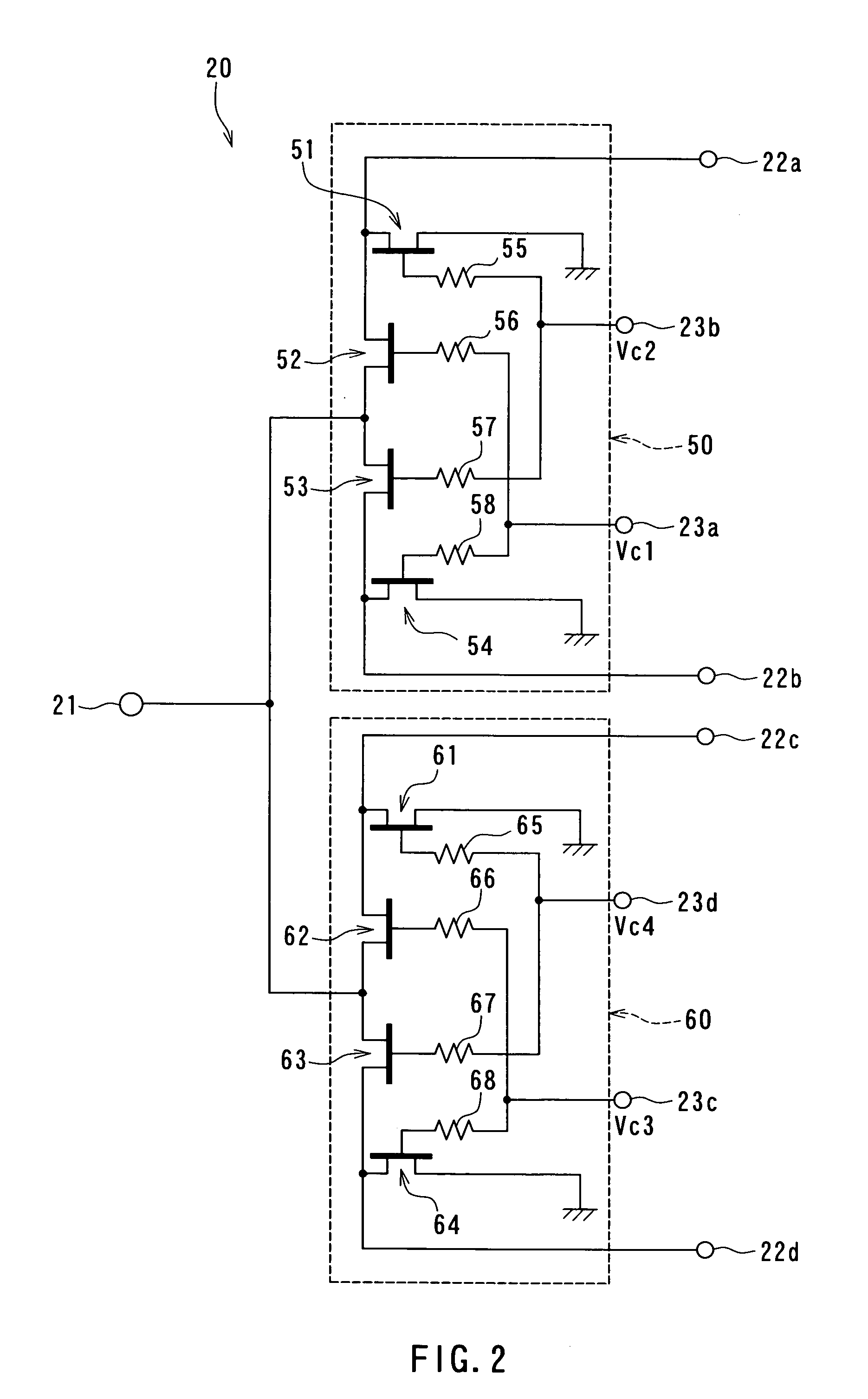
[0038]The high frequency switch module 1 comprises: an antenna port 2 connected to an antenna not shown; transmission signal ports 3 and 4; reception signal ports 5 and 6; a high frequency switch 20; and two low-pass filters (hereinafter ca...


PUM


Abstract

A high frequency switch module comprises an antenna port, a plurality of transmission signal ports, a plurality of reception signal ports, a high frequency switch, a plurality of LPFs and a plurality of phase adjusting lines. The high frequency switch allows one signal port among the transmission signal ports and the reception signal ports to be selectively connected to the antenna port. The high frequency switch includes a field-effect transistor made of a GaAs compound semiconductor. Each of the phase adjusting lines connects the high frequency switch to each of the LPFs. Each of the phase adjusting lines adjusts a phase difference between a progressive wave of a harmonic resulting from a transmission signal and produced at the high frequency switch and a reflected wave resulting from reflection of the progressive wave from each of the LPFs such that the power of a composite wave made up of the progressive wave and the reflected wave is made lower at the point of the high frequency switch.

Description

BACKGROUND OF THE INVENTION[0001]1. Field of the Invention[0002]The present invention relates to a high frequency switch module used for switching frequency bands and switching between transmission signals and reception signals, for example, of a radio communications device such as a cellular phone, and to a multi-layer substrate used for such a high frequency switch module.[0003]2. Description of the Related Art[0004]Cellular phones operable in multiple frequency bands have been practically utilized. For example, cellular phones for the global system for mobile communications (GSM) started as phones operable in a single band of the extended GSM (EGSM), and has been converted to phones operable in dual bands of the EGSM and the digital cellular system (DCS), and to phones operable in triple bands of the EGSM, the DCS, and the personal communications service (PCS). The number of frequency bands in which a single cellular phone is operated is thereby increased to extend the speech cha...

Claims


Application Information

Patent Timeline
Patent Type & Authority Patents(United States)
IPC IPC(8): H04B1/44H04B1/46H04B7/00H01P1/15H01P1/212
CPCH01P1/15H01P1/212
Inventor ITAKURA, MASAMIGOI, TOMOYUKIADACHI, TAKUYA
Owner SNAPTRACK
Why Eureka
Try Eureka