Non-volatile semiconductor memory device allowing shrinking of memory cell

a semiconductor memory and non-volatile technology, applied in the direction of bulk negative resistance effect devices, instruments, basic electric elements, etc., can solve the problems of inability to accurately perform data writing and reading, inability to write and read data correctly, and longer access time, so as to reduce the size of the memory cell

Inactive Publication Date: 2007-04-24
RENESAS ELECTRONICS CORP
View PDF14 Cites 208 Cited by
  • Summary
  • Abstract
  • Description
  • Claims
  • Application Information

AI Technical Summary

Benefits of technology

[0029]An object of the present invention is to provide a non-volatile semiconductor memory device and non-vo

Problems solved by technology

There is a problem that the access time becomes longer.
There is a problem that data writing and reading cannot be performed correctly.
Thus, there is a similar problem that data writing and reading cannot be performed accurately.
In such a case, the problem of potential distribution on word line WL and collector line CK caused by diffusion resistance Rpw and substrate res

Method used


Image

  • Non-volatile semiconductor memory device allowing shrinking of memory cell
  • Non-volatile semiconductor memory device allowing shrinking of memory cell
  • Non-volatile semiconductor memory device allowing shrinking of memory cell

Examples


first embodiment

[0101

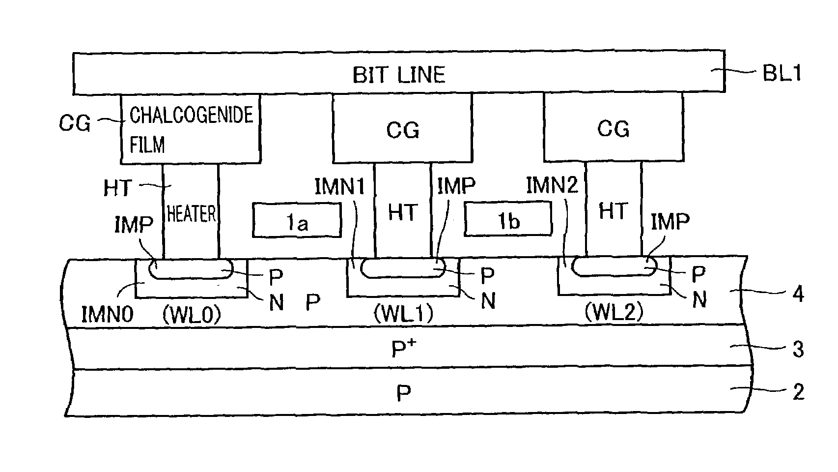
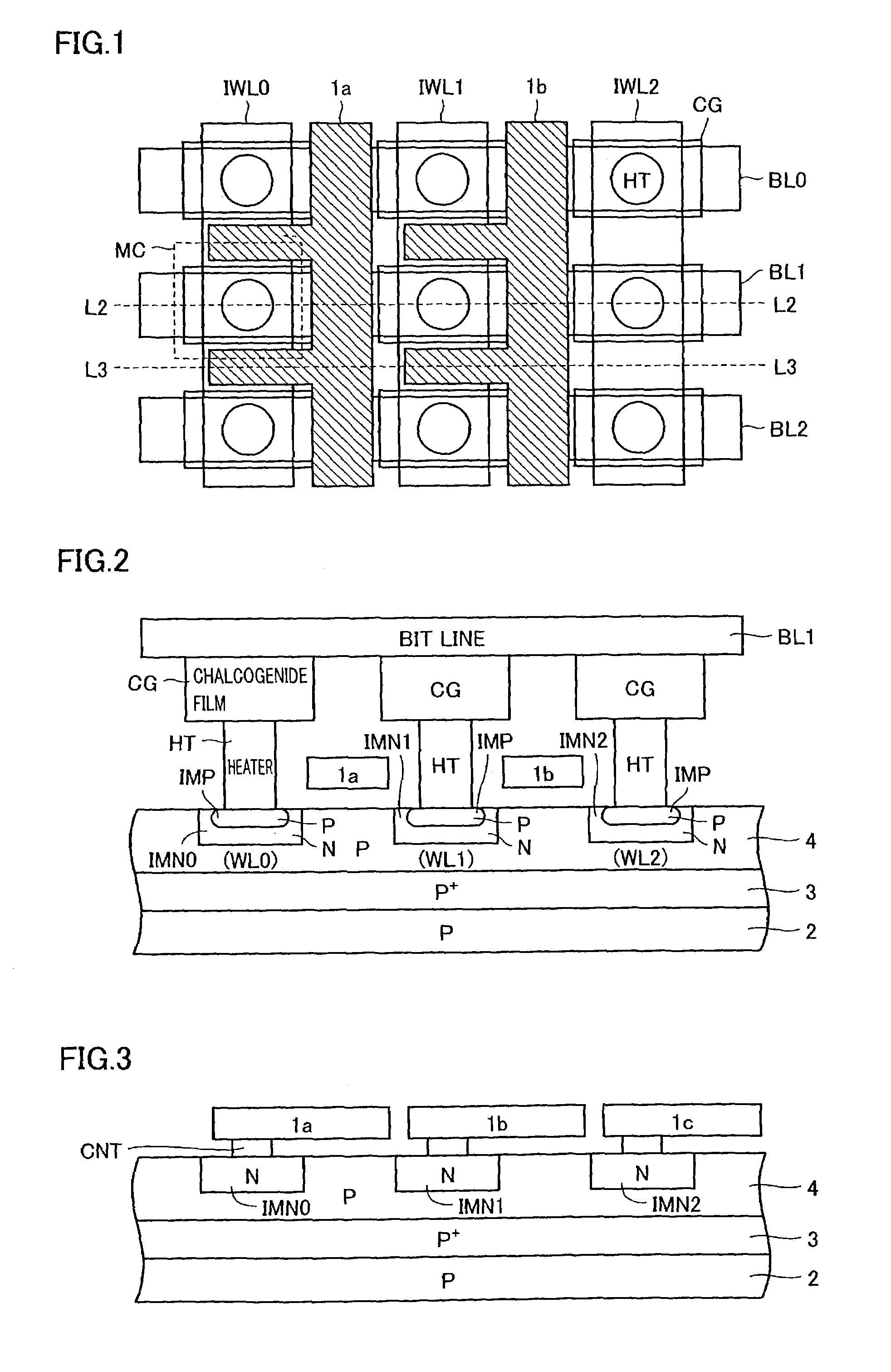
[0102]FIG. 1 schematically shows the layout of the memory array of a non-volatile semiconductor memory device according to a first embodiment of the present invention. FIG. 1 shows the layout of memory cells MC arranged in three rows and three columns. Referring to FIG. 1, word lines WL0–WL2 are provided corresponding to the respective rows of memory cells MC, and bit lines BL0–BL2 are disposed corresponding to the respective columns of memory cells MC, as in the conventional example. Word lines WL0–WL2 are each formed of an impurity layer located at the surface of a semiconductor substrate. Word lines WL0–WL2 each extend continuously in the row direction.

[0103]Memory cell MC includes a chalcogenide film CG of a rectangular feature coupled to bit line BL (indicating generically BL0–BL2), a heater HT for heating chalcogenide film CG, and a transistor element formed between this heater and a substrate region not shown. In FIG. 1, the transistor element included in memory cell MC ...

second embodiment

[0141

[0142]FIG. 8 schematically shows an arrangement of the array of a non-volatile semiconductor memory device according to a second embodiment of the present invention. FIG. 8 shows memory cells MC arranged in three columns and three rows representatively, either. N type impurity layers 30a–30c functioning as word lines are formed corresponding to the respective rows of memory cells MC and extending continuously in the row direction. Conductive layers 32a–32c are formed extending continuously in the column direction so as to cross impurity layers 30a–30c, respectively. Conductive layers 32a–32c function as bit lines BL.

[0143]Memory cell MC includes a phase change element 33 with a chalcogenide film, and a heater element 34 with a heater that heats the chalcogenide film of phase change element 33. In each memory cell MC, phase change element 33 has a width in a row direction substantially identical to that of conductive layers (bit line conductive layer) 32a–32c that function as bi...

third embodiment

[0199

[0200]FIG. 19 schematically shows an entire construction of a non-volatile semiconductor memory device according to a third embodiment of the present invention. Referring to FIG. 19, the non-volatile semiconductor memory device includes a memory cell array 100 having memory cells MC arranged in rows and columns. Memory cell MC includes a variable resistance element with a phase change element, and a select transistor for selecting this variable resistance element.

[0201]In memory cell array 100, a word line WL is disposed corresponding to a row of memory cells MC. Corresponding to each column of memory cells MC, a bit line BL is disposed. Moreover, dummy cells DMCa and DMCb are arranged in alignment with each row of memory cells MC. A dummy cell DMCa is connected to a dummy bit line DBLa, and a dummy cell DMCb is connected to a dummy bit line DBLb. Memory cell MC and dummy cells DMCa and DMCb are connected to one word line WL. Dummy cells DMCa and DMCb store data complementary t...


PUM


Abstract

Dummy cells are disposed in alignment with memory cells arranged in rows and columns in a memory array. The memory cell includes a variable resistance element and a select transistor having a collector connected to a substrate region and selecting the variable resistance element in response to a row select signal. Corresponding to a row of memory cells, there is provided a word line connecting to memory cells on corresponding row and transmitting the row select signal, and a word line shunting line electrically connected at predetermined intervals to each word line. Moreover, corresponding to a row of dummy cells and a column of dummy cells, there is provided substrate shunt lines electrically connected to the substrate region. The voltage distribution in the substrate region is eliminated to achieve stable operating characteristics of the memory cell transistor. In addition, a word line is driven at high speed by a word line shunt structure.

Description

BACKGROUND OF THE INVENTION[0001]1. Field of the Invention[0002]The present invention relates to non-volatile semiconductor memory devices, particularly to a phase change memory in which the crystalline state changes according to the stored data. More specifically, the present invention relates to the technique for shrinking the components of a phase change memory.[0003]2. Description of the Background Art[0004]A non-volatile memory that stores data in a non-volatile manner is known as one type of a semiconductor memory device. Since data is stored in a non-volatile manner in such a non-volatile memory, data can be retained even if power is cut off. No power supply for data retention is required. Thus, non-volatile memories are widely utilized in various applications such as portable equipment.[0005]As such a non-volatile memory, a magnetic memory that utilizes the magneto-resistance effect is known, in which the magnetic substance has a different resistance depending upon the direc...

Claims


Application Information

Patent Timeline
IPC IPC(8): H01L47/00H01L27/10H01L29/06G11C13/00G11C5/02G11C7/14G11C16/02H01L27/105H01L27/24
CPCG11C5/02G11C7/14G11C13/0004H01L27/24H10B63/00
Inventor OOISHI, TSUKASA
Owner RENESAS ELECTRONICS CORP
Why Eureka
Try Eureka