
Floating body cell dynamic random access memory with optimized body geometry

a floating body cell and random access memory technology, applied in the direction of semiconductor devices, electrical equipment, transistors, etc., can solve the problems of reducing the speed of peripheral circuits and logic circuits, scaling limitations of drams, and increasing manufacturing costs

Inactive Publication Date: 2007-04-24
KK TOSHIBA
View PDF11 Cites 6 Cited by
  • Summary
  • Abstract
  • Description
  • Claims
  • Application Information

AI Technical Summary

Benefits of technology

The invention relates to a semiconductor device and a method of manufacturing it. The semiconductor device includes a semiconductor layer insulated from a support substrate by a first insulation layer, with a source region and a drain region formed in the semiconductor layer. A second insulation layer is formed on the body region between the source and drain regions, with a word line and a bit line electrically connected to the drain region. The area of the body region in contact with the first insulation layer is larger than the area in contact with the second insulation layer. The method of manufacturing the semiconductor device includes preparing an SOI substrate, forming a mask material, patterning the mask material, etching the semiconductor layer, and forming a third insulation layer. The technical effects of the invention include improving the stability and reliability of the semiconductor device, and reducing the size of the device.

Problems solved by technology

Therefore, 1T-1C DRAMs have a scaling limitation.
Further, since 1T-1C DRAMs need capacitors, their manufacturing process is complicated, increasing their manufacturing cost.
However, simply thinning the BOX layer invites an increase of the parasitic capacitance between the SOI layer region and the support substrate in peripheral circuits and logic circuits.
Increase of the parasitic capacitance decreases the speed of peripheral circuits and logic circuits, and increases their power consumption.

Method used


Image

  • Floating body cell dynamic random access memory with optimized body geometry
  • Floating body cell dynamic random access memory with optimized body geometry
  • Floating body cell dynamic random access memory with optimized body geometry

Examples


first embodiment

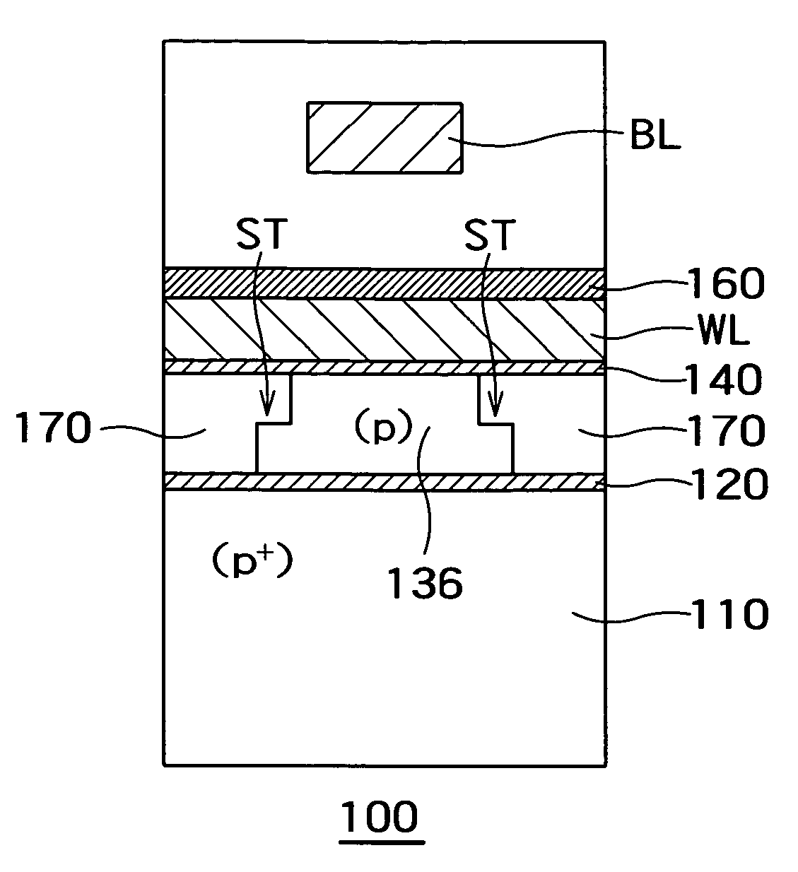
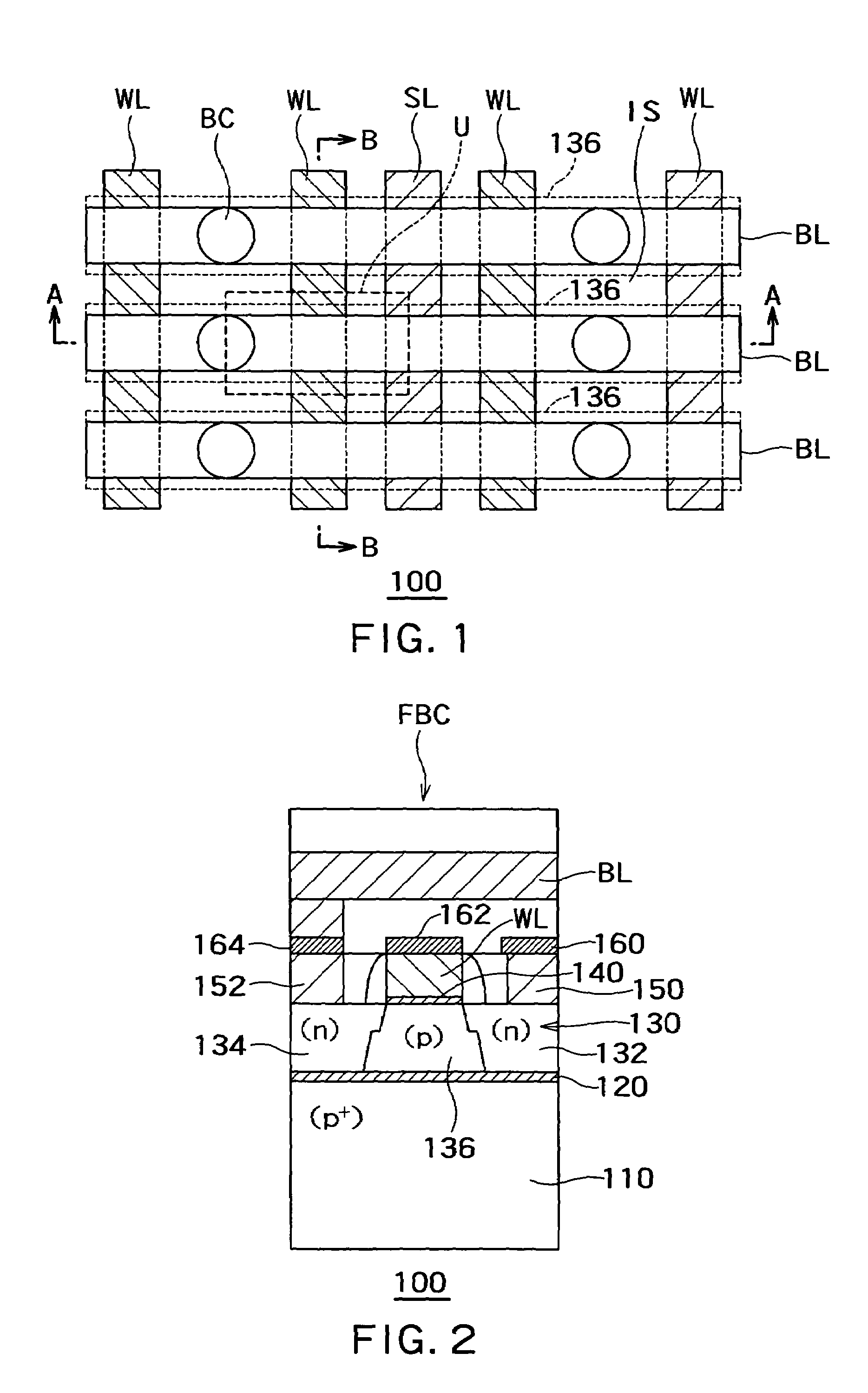
[0036]FIG. 1 is a plan view of DRAM 100 according to the first embodiment of the invention. In this embodiment, a peripheral circuit for controlling the DRAM 100 may be provided around the DRAM 100. The DRAM 100 includes word lines WL, bit lines BL and source lines SL. The word lines WL and the source lines SL extend approximately in parallel whereas the bit lines BL extend in directions approximately perpendicular to the word lines WL and the source lines SL. Bit contacts BC make electrical connection between the bit lines BL and the drain regions below the bit lines BL (see FIG. 2).

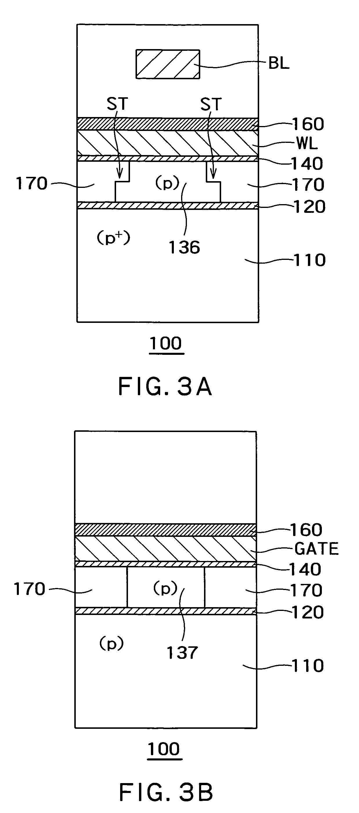
[0037]FIG. 2 is a cross-sectional view of a unit cell U taken along the A—A line of FIG. 1. Fig. 3A is a cross-sectional view of the unit cell U taken along the B—B line of FIG. 1, and FIG. 3B is a cross-sectional view of a peripheral logic circuit. First referring to FIG. 2, the DRAM 100 further includes a BOX layer 120, an SOI layer 130, and a p+type semiconductor substrate having impurity concentrati...

second embodiment

[0074]FIG. 15 is a plan view of DRAM 300 according to the second embodiment of the invention. Configuration of body regions 336 of the second embodiment is different from that of the body regions 136 in the first embodiment. The body regions 336 do not have steps ST (see FIG. 3A) on their sidewalls in the regions corresponding to bit line contacts BC. In the other regions not corresponding to the bit line contacts BC, the body regions 336 have steps on their sidewalls. The other components of the second embodiment may be identical to corresponding components of the first embodiment.

[0075]A cross-sectional view of a unit cell U shown in FIG. 15 taken along a bit line (A—A line) appears identically to FIG. 2, and a cross-sectional of the unit cell U taken along a word line WL (B—B line) appears identically to FIG. 3A. However, a cross-sectional view taken along a portion of bit line contacts BC (C—C line) appears differently from the first embodiment.

[0076]FIG. 16 is the cross-section...


PUM


Abstract

A semiconductor device includes a semiconductor substrate; a first insulation layer formed on the semiconductor substrate; a semiconductor layer insulated from the semiconductor substrate by the insulation layer; a source region of a first conduction type and a drain region of the first conduction type formed in the semiconductor layer; a body region of a second conduction type formed in the semiconductor layer between the source region and the drain region, said body region being capable of storing data by accumulating or releasing electric charge; a second insulation layer formed on the body region; a word line formed on the second insulation layer and insulated from the body region by the second insulation layer; and a bit line electrically connected to the drain region, wherein the area of the body region in contact with the first insulation layer is larger than the area thereof in contact with the second insulation layer.

Description

CROSS-REFERENCE TO RELATED APPLICATIONS[0001]This application is based upon and claims the benefit of priority from the prior Japanese Patent Application No. 2003-392342, filed on Nov. 21, 2003, the entire contents of which are incorporated herein by reference.BACKGROUND OF THE INVENTION[0002]1. Field of the Invention[0003]The present invention relates to a semiconductor device and a method of manufacturing a semiconductor device.[0004]2. Related Background Art[0005]Semiconductor storage devices including DRAMs are more and more down-scaled in recent years. 1T-1C (1 transistor-1 capacitor) type DRAMs, however, need a certain area for capacitors to secure the storage capacitance of the capacitors. Therefore, 1T-1C DRAMs have a scaling limitation. Further, since 1T-1C DRAMs need capacitors, their manufacturing process is complicated, increasing their manufacturing cost.[0006]To cope with this problem, techniques for forming DRAMs on an S0I (silicon on insulator) substrate have been de...

Claims


Application Information

Patent Timeline
Patent Type & Authority Patents(United States)
IPC IPC(8): H01L29/06H01L27/10H01L21/8242H01L21/84H01L27/108H01L27/12
CPCH01L21/84H01L27/108H01L27/10844H01L27/10894H01L27/10897H01L27/1203H01L29/7841H10B12/00H10B12/01H10B12/09H10B12/50
Inventor SHINO, TOMOAKI
Owner KK TOSHIBA
Learn More