Semiconductor device for controlling switching power supply

a technology of switching power supply and semiconductors, which is applied in the direction of pulse generators, instruments, pulse techniques, etc., can solve the problems of increasing the overall cost of the circuitry, and reducing the power efficiency of the switching power supply, so as to reduce the switching loss, suppress high-frequency operation under light loads, and improve the power supply efficiency under light loads

Inactive Publication Date: 2007-04-24
COLLABO INNOVATIONS INC
View PDF12 Cites 17 Cited by
  • Summary
  • Abstract
  • Description
  • Claims
  • Application Information

AI Technical Summary

Benefits of technology

[0021]In order to resolve the above-described problems of the prior art, an object of this invention is to provide a semiconductor device for controlling switching power supply able to suppress high-frequency operation under light loads to reduce switching losses, improve power supply efficiency under light loading, and reduce power consumption under light loading.
[0026]As a result, high-frequency operation under light loads can be suppressed to reduce switching losses, and the power supply efficiency under light loads can be improved, reducing power consumption under light loading. In addition, because of quasi-resonant operation, higher efficiency and lower noise can easily be realized over the entire load range from light loads to heavy loads, even during normal operation.

Problems solved by technology

Such power supply systems have the defect that two switching power supply devices (converters) are necessary, entailing increase overall costs of the circuitry, including the semiconductor devices for controlling switching power supply.
Hence even when there is no load, losses occur due to the switching operation in switching elements, and the lighter the load, the greater is the fraction of such losses in switching elements.
Consequently the power efficiency of the switching power supply is reduced, and so there is the problem that the desire for reduced power consumption when the power supply is in standby cannot be realized.
Further, in a partial resonance-type switching power supply the oscillation frequency rises under light loads, so that switching losses are increased, and there is the problem that the power supply efficiency is lowered in standby mode.
In this switching power supply, the oscillation frequency during intermittent switching operation is fixed regardless of the load state, and so this solution is far from adequate with respect to improvement of the power supply efficiency during standby.
However, because a conventional switching power supply such as that described above is under RCC control, the lighter the load on the secondary-windings side of the transformer, the higher is the switching frequency, so that there are the problems that the switching loss per unit time in the switching element 1 increases, and that during light loading such as in standby mode the power supply efficiency is worsened.

Method used


Image

  • Semiconductor device for controlling switching power supply
  • Semiconductor device for controlling switching power supply
  • Semiconductor device for controlling switching power supply

Examples


embodiment 1

(Embodiment 1)

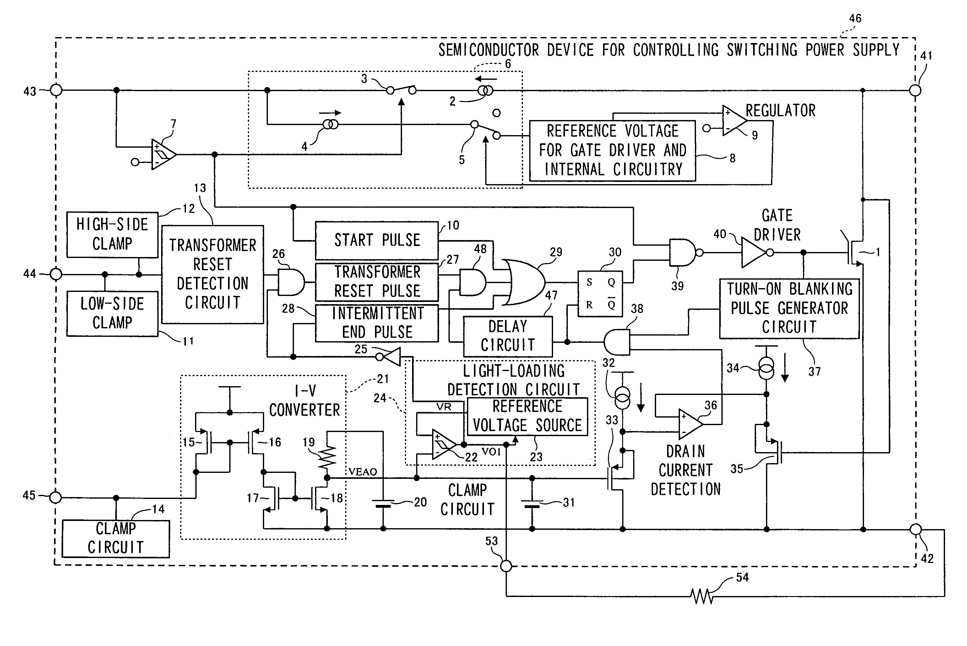
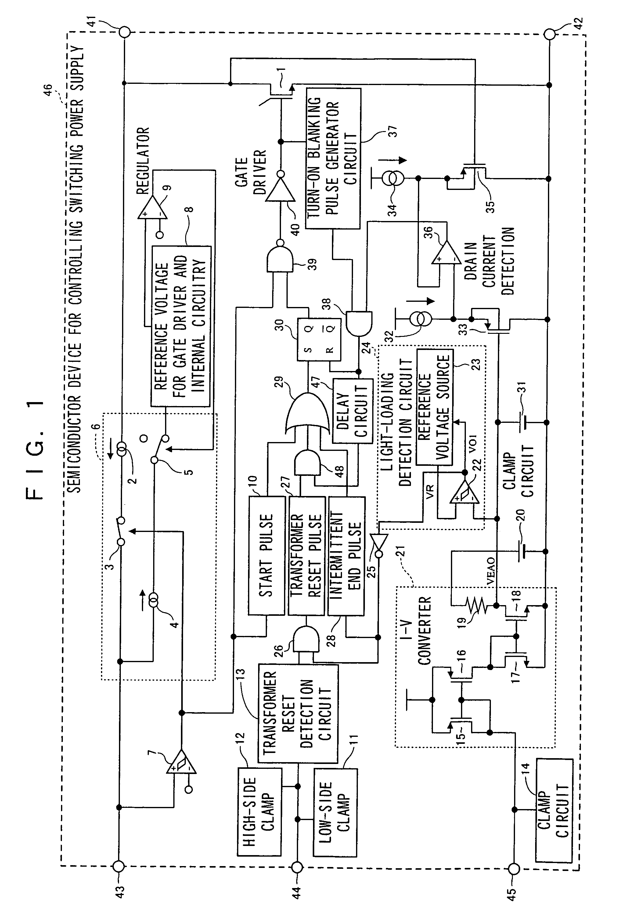
[0044]The semiconductor device for controlling switching power supply of Embodiment 1 of the invention is explained.

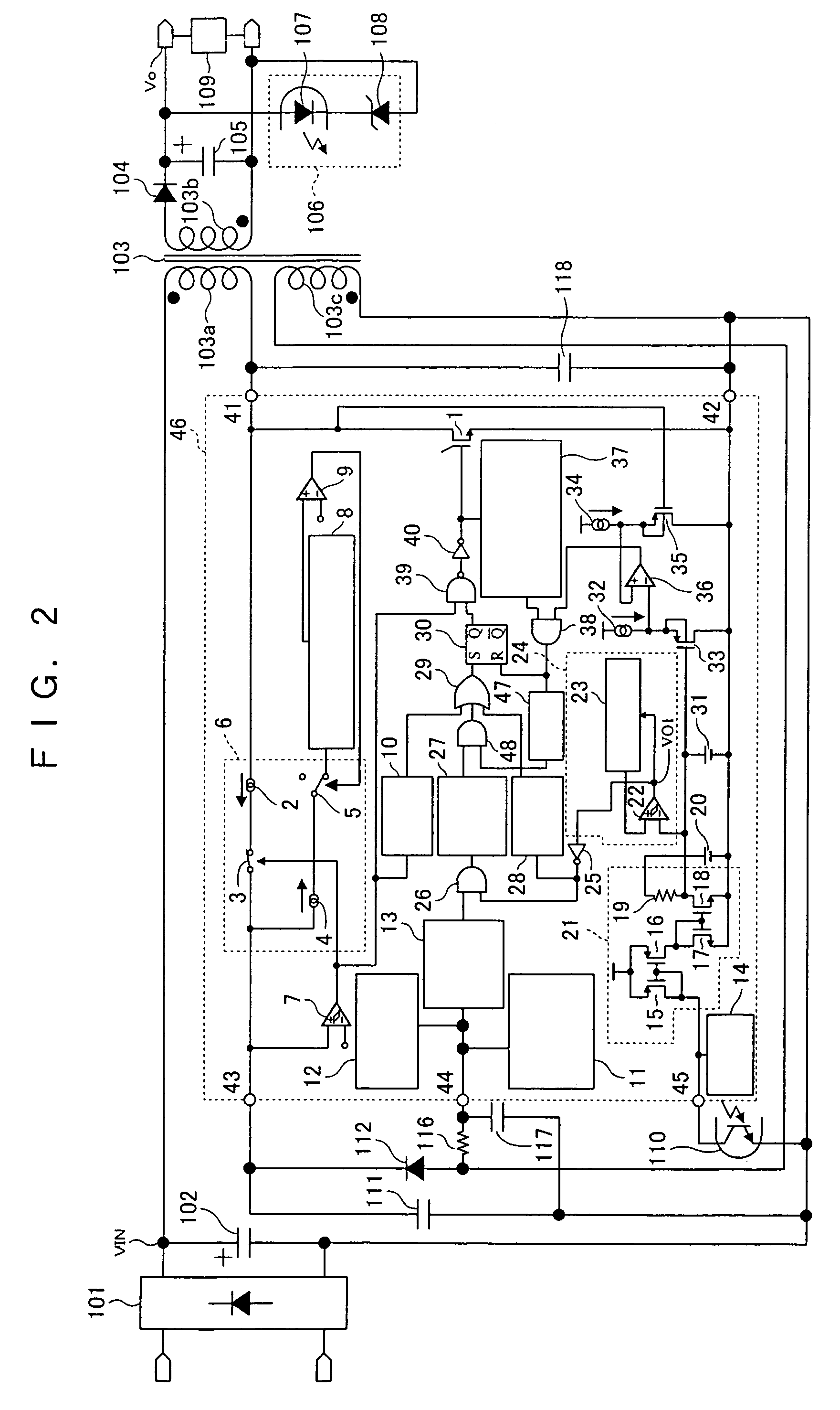
[0045]FIG. 1 is a circuit diagram showing one configuration example of the semiconductor device for controlling switching power supply of Embodiment 1 of the invention. FIG. 2 is a circuit diagram showing one configuration example of a switching power supply device comprising the semiconductor device for controlling switching power supply of Embodiment 1.

[0046]The semiconductor device for controlling switching power supply 46 shown in FIG. 1 is provided with a light-loading detection circuit 24, to which is provided the output voltage VEAO resulting from voltage conversion by the I-V converter 21 of the current flowing from the control terminal 45. In this light-loading detection circuit 24 is provided a light-loading detection comparator 22. As the negative input of the light loading detection comparator 22, the output voltage VEAO output from the I-V co...

embodiment 2

(Embodiment 2)

[0109]The semiconductor device for controlling switching power supply of Embodiment 2 of the invention is explained.

[0110]FIG. 9 is a circuit diagram showing one configuration example of a semiconductor device for controlling switching power supply of Embodiment 2. FIG. 10 is a circuit diagram showing another configuration example of the semiconductor device for controlling switching power supply of this Embodiment 2.

[0111]In the semiconductor device for controlling switching power supply 46, as shown in FIG. 9, a terminal 50 connected to the delay circuit 47 is provided, and a capacitor 51 is connected externally between this terminal 50 and a terminal (ground, GND) 42.

[0112]In this configuration, the capacitor 51 connected externally between the terminal 50 and the terminal 42 is used as the charging capacitance C of the delay circuit 47 shown in FIG. 7.

[0113]In this case also, an advantageous result similar to that of the semiconductor device for controlling switchi...

embodiment 3

(Embodiment 3)

[0115]The semiconductor device for controlling switching power supply of Embodiment 3 of the invention is explained.

[0116]FIG. 11 is a circuit diagram showing one configuration example of a semiconductor device for controlling switching power supply of Embodiment 3 of the invention. FIG. 12 is a circuit diagram showing one configuration example of the delay circuit in the semiconductor device for controlling switching power supply of this Embodiment 3. FIG. 13 is a waveform diagram showing operation in the delay circuit in the semiconductor device for controlling switching power supply of this Embodiment 3. And, FIG. 14 is a circuit diagram showing another configuration example of the semiconductor device for controlling switching power supply of Embodiment 3.

[0117]FIG. 11 shows an example in which the delay circuit 47 in the semiconductor device for controlling switching power supply of Embodiment 1 shown in FIG. 1 is configured such that the delay time is automatical...


PUM


Abstract

In a semiconductor device for controlling switching power supply of this invention, having a switching element and switching operation control circuit, after receiving a current detection signal when switching is turned off, a fixed delay time is applied to the current detection signal by a delay circuit so that switching turn-on control by a transformer reset pulse signal obtained based on a signal from the tertiary windings of the transformer is not accepted within a blanking time corresponding to the delay time. Thus, the switching by the switching element is halted.

Description

BACKGROUND OF THE INVENTION[0001]1. Field of the Invention[0002]This invention relates to a semiconductor device for controlling switching power supply, which controls the output voltage of a switching power supply through switching operation.[0003]2. Description of the Related Art[0004]Switching power supply devices, which use switching power supply semiconductor devices to control (stabilize and similar) an output voltage by utilizing the switching operation of semiconductors (transistors or other switching elements), have come to be widely used as the power supplies of home appliances and other equipment for home use, for the purpose of improving power efficiency through reduced power consumption and similar.[0005]In recent years in particular, attention has been paid to reduction of power consumption through operation idling (standby) in home appliances and other equipment, from the standpoint of measures to prevent global warming, and there have been strong demands for switchin...

Claims


Application Information

Patent Timeline
Patent Type & Authority Patents(United States)
IPC IPC(8): H03K3/023H02M3/335H02M3/28H03B1/00
CPCH02M3/33507H02M3/33523C02F1/482
Inventor YAMASHITA, TETSUJI
Owner COLLABO INNOVATIONS INC
Why Eureka
Try Eureka