
Optical device and three-dimensional display device

a three-dimensional display and optical device technology, applied in optics, instruments, electrical devices, etc., can solve the problems of affecting the speed of the resumption of driving, the delay of the resumption timing upon driving by several seconds, and the inability to improve the resumption timing. , to achieve the effect of high speed

Inactive Publication Date: 2007-04-24
NIPPON TELEGRAPH & TELEPHONE CORP
View PDF20 Cites 110 Cited by
  • Summary
  • Abstract
  • Description
  • Claims
  • Application Information

AI Technical Summary

Benefits of technology

The present invention provides an optical device that can be driven at high speed, achieve high uniformity, and vary an optical property sequentially, periodically, and uniformly. The device includes a layer of transparent material with a curved surface configuration, a layer of variable refractive index material with dielectric constant anisotropy, and at least two transparent electrodes. The device can be easily fabricated and is not influenced by the surface configuration of the transparent material layer. The device can also be used for realizing an active mirror or various other types of optical devices. The invention also provides a three-dimensional display device for forming a three-dimensional image from two-dimensional images.

Problems solved by technology

The kinds of active optical devices whose optical properties can be varied by voltage or the like are quite limited.
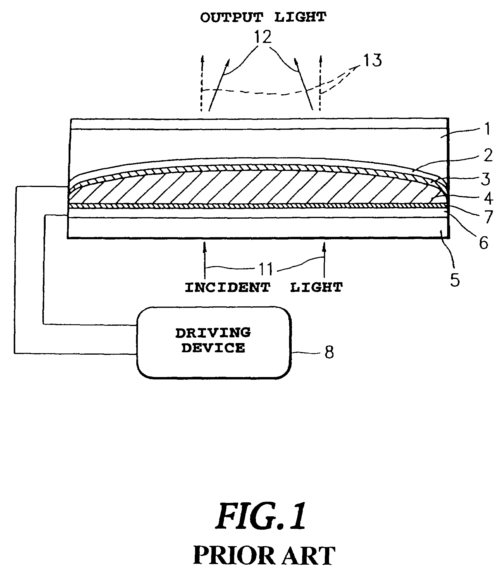
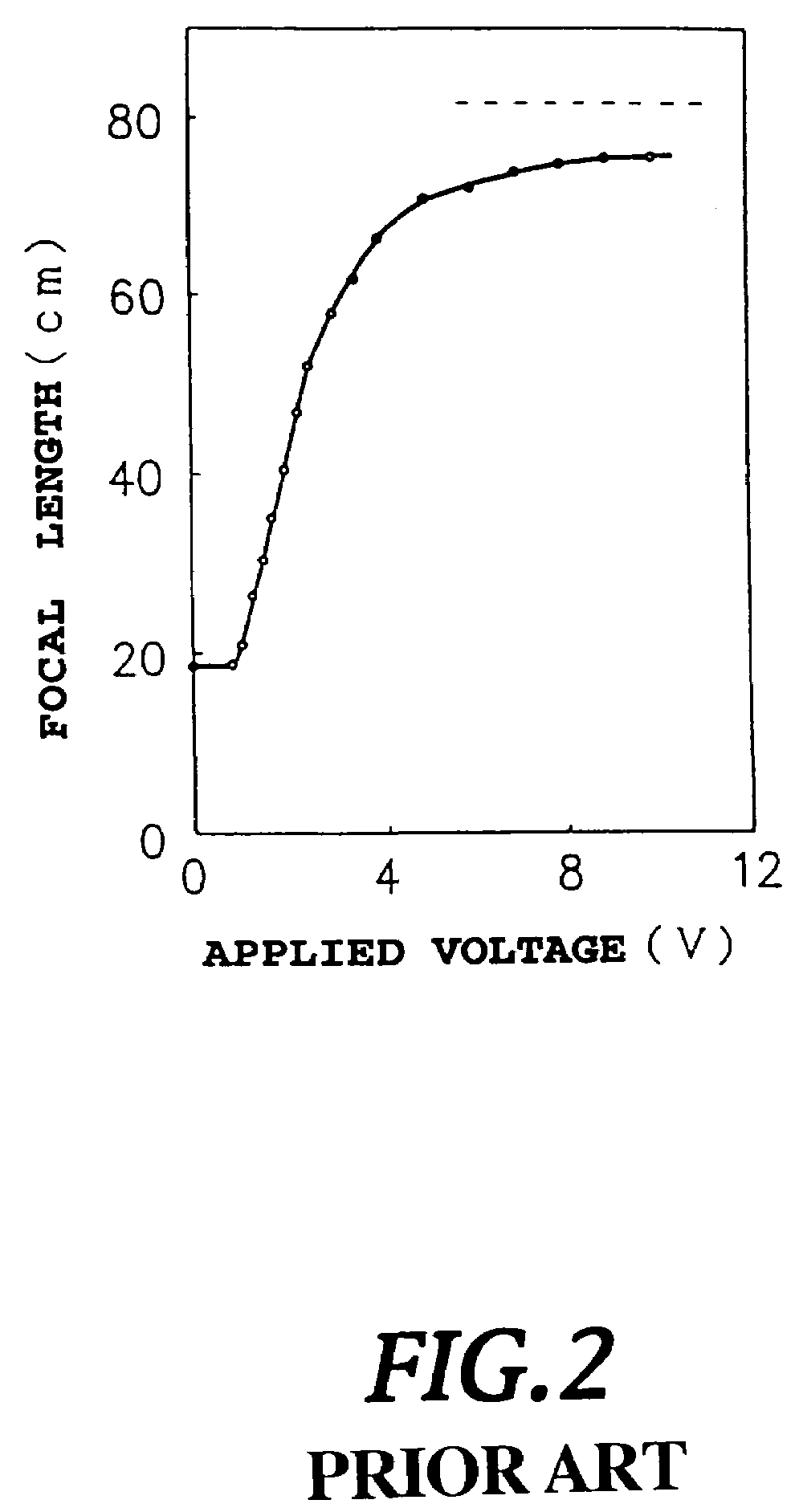
In such a optical device, since the liquid crystal 4 has a large thickness of several hundreds μm or more, a drawback has been encountered in that a resumption timing upon driving is delayed significantly by several seconds, as shown in FIG. 3.
Furthermore, even if the applied voltage is increased, the resumption timing can be hardly improved.
Therefore, currently, there is no effective method for shortening a resumption period.
Furthermore, there is a disadvantage in that distribution of the variation amount of the optical property depends on the position with respect to the lens.
Furthermore, in the case where the surface configuration of the planar concave lens 1 is more complicated, particularly when it has deep grooves or sharp projections, it becomes difficult to uniformly form the transparent electrode, so that a circuit breakage or high resistance is liable to occur.
Additionally, in such case, an alignment process of the alignment layers for aligning the liquid crystal, such as a rubbing process and the like, becomes difficult.
Despite this fact, since an equal voltage is applied to all positions of the transparent electrodes, degradation of insulation, short circuits, etc. are liable to occur in a narrow region.
As set forth above, the conventional active optical device employing a material having a variable refractive index encounters various practical drawbacks or shortcoming in production and driving.

Method used


Image

  • Optical device and three-dimensional display device
  • Optical device and three-dimensional display device
  • Optical device and three-dimensional display device

Examples


third embodiment

of Three-Dimensional Display Device

[0320]FIG. 45 is a block diagram illustrating a schematic construction of a third embodiment of the three-dimensional display device according to the present invention. Reference numeral 151 denotes a projection type display; 152, a shutter; 153, a scattering plate; 154, an image recording and reproducing apparatus; and 155, a synchronization control device.

[0321]In FIG. 45, the projection type display 151 has been well known. In the third embodiment, a plurality of displays are employed for lowering a depiction speed of the respective projection type displays.

[0322]The shutters 152 are provided in the respective projection type displays 151, for projecting images from each of projection type displays 151 on the scattering plate 153 in a time division manner.

[0323]The scattering plate 153 is of a known type for displaying the image projected from the projection type display 151. For example, the scattering plate 152 is placed within the focal lengt...

fourth embodiment

of Three-Dimensional Display Device

[0343]With the three-dimensional display devices in the foregoing embodiments, since the two-dimensional images sampled in the depth direction are displayed in time division to be thus integrated into the three-dimensional image by an after image effect, it is impossible to avoid a phantom phenomenon, which allows the back side or inside of the object which should be hidden from the observer's sight to be viewed transparently. This is an immense obstacle to reproduction of the natural three-dimensional image, and is the reason why the three-dimensional display devices in the foregoing embodiments are used only for reproducing wire frame like images. Hereinafter, a three-dimensional display device capable of avoiding the above-stated drawback will be described with reference to FIGS. 49 to 59.

[0344]FIG. 49 is a schematic view showing a construction of the fourth embodiment of the three-dimensional display device according to the invention, and FIG. ...

fifth embodiment

of Three-Dimensional Display Device

[0358]The fourth embodiment as set forth above uses one example according to the present invention, in which the three-dimensional image is a real image. It is also possible to avoid the phantom phenomenon even if the three-dimensional image is a virtual image. In the fifth embodiment, a description will be given on a varifocal lens type device as a phantom three-dimensional display device in which a phantom three-dimensional image is reproduced as a virtual image. The fifth embodiment of the three-dimensional display device will be discussed hereinafter with reference to FIGS. 51 and 52.

[0359]FIG. 51 is a view showing a schematic construction of the fifth embodiment of the three-dimensional display device according to the present invention, and FIG. 52 is an illustration for explaining basic operation of the fifth embodiment of the three-dimensional display device for avoiding a phantom phenomenon.

[0360]In FIGS. 51 and 52, reference numeral 202 de...


PUM

PropertyMeasurementUnit
frequencyaaaaaaaaaa
dielectric constantaaaaaaaaaa
refractive indexaaaaaaaaaa

Abstract

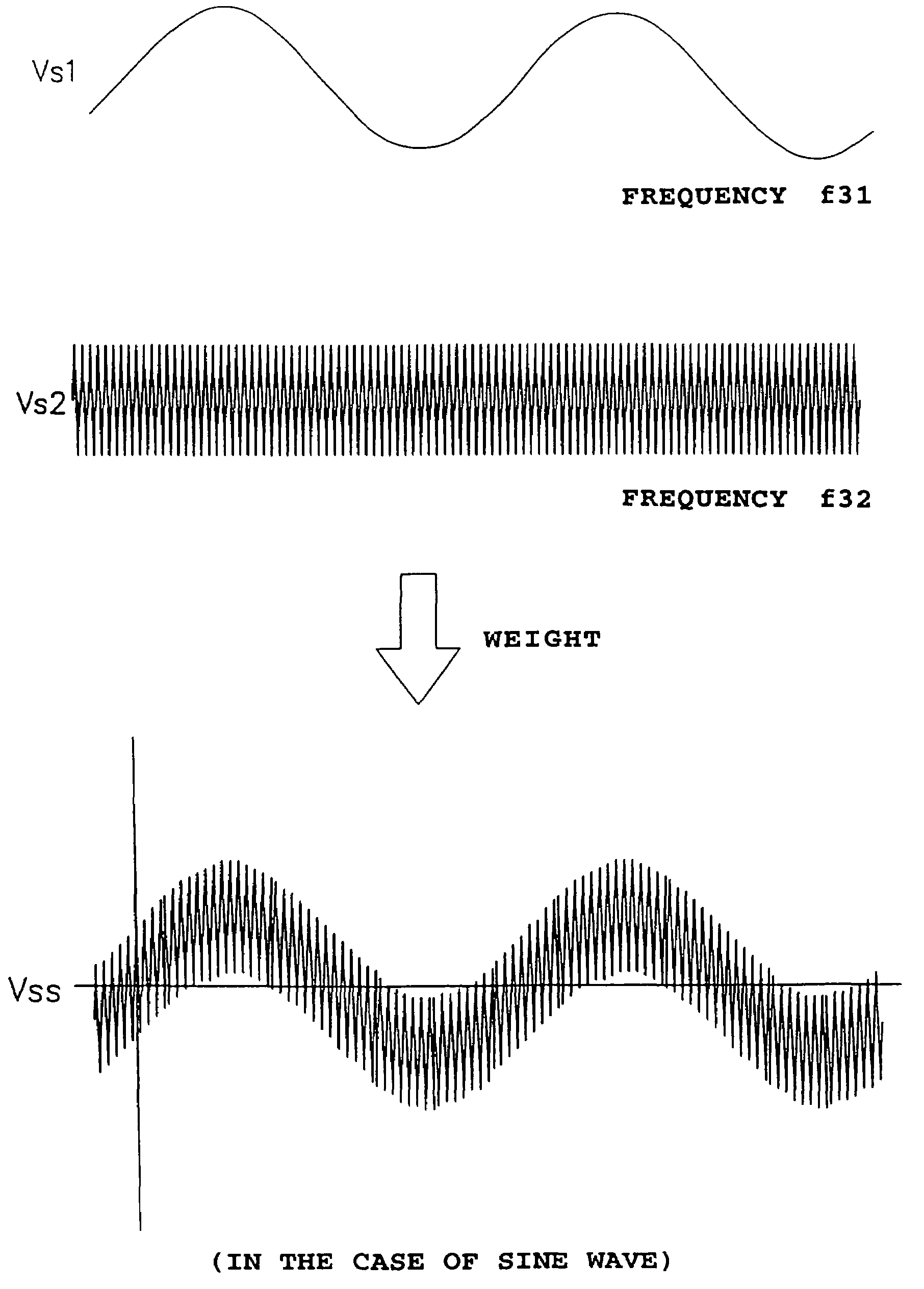
An optical device includes a transparent material layer having a desired curved surface configuration, a layer including a variable refractive index material having a dielectric constant anisotropy, at least two transparent electrodes arranged to sandwich the transparent material layer and the variable refractive index material, and a driving device supplying a voltage including driving frequencies f1 and f2 between the transparent electrodes. The difference Δ∈ in the dielectric constant of the variable refractive index material due to the anisotropy is positive at one of the driving frequencies and negative at the other driving frequency.

Description

CROSS REFERENCE TO RELATED APPLICATIONS[0001]This application is a divisional application of application Ser. No. 10 / 011,638 filed Dec. 11, 2001 now U.S. Pat. No. 6,714,174, which is a divisional application of application Ser. No. 08 / 784,353, filed on Jan. 16, 1997 now U.S. Pat. No. 6,469,683. The disclosure of the above-referenced patent applications, as well as that of each U.S. and foreign patent and patent application identified in the specification of the present application, is incorporated herein by reference.BACKGROUND OF THE INVENTION[0002]1. Field of the Invention[0003]The present invention relates to an optical device which can periodically or sequentially vary an optical property of the optical device, such as the focal length of a lens, the deflection angle of a prism, the divergence angle of a lenticular lens and so on.[0004]Further, the present invention relates to a three-dimensional display device and its driving method. More specifically, the present invention rel...

Claims


Application Information

Patent Timeline
Patent Type & Authority Patents(United States)
IPC IPC(8): G09G3/00G02B27/22G02F1/1333G02F1/139G02F1/29H04N13/239
CPCG02B27/2271G02B27/2278G02F1/1333G02F1/29H04N13/0239H04N13/0418H04N13/042H04N13/0422H04N13/044H04N13/0495H04N13/0497G02F1/1392G02F2001/294H04N13/0048H04N13/0055H04N13/0404H04N13/0438H04N13/341H04N13/305H04N13/395H04N13/32H04N13/344H04N13/189H04N13/324H04N13/161H04N13/239H04N13/322H04N13/398G02B30/50G02B30/52G02F1/294
Inventor SUYAMA, SHIRODATE, MUNEKAZUKOHDA, SHIGETOKATO, KINYASAKAI, SHIGENOBU
Owner NIPPON TELEGRAPH & TELEPHONE CORP
Learn More