Laser assisted direct imprint lithography

a technology of imprint lithography and laser, which is applied in the field of imprint lithography, can solve the problems of increasing optical lithography difficulty, limited resolution by light wavelength, and relatively slow steps in developing and removing resists

Inactive Publication Date: 2007-05-01
PRINCETON UNIV
View PDF43 Cites 37 Cited by
  • Summary
  • Abstract
  • Description
  • Claims
  • Application Information

AI Technical Summary

Problems solved by technology

A difficulty with this process is that resolution is limited by the wavelength of the light, scattering in the resist and substrate, and the thickness and properties of the resist.
As a consequence optical lithography becomes increasingly difficult as desired feature size becomes smaller.

Method used


Image

  • Laser assisted direct imprint lithography
  • Laser assisted direct imprint lithography
  • Laser assisted direct imprint lithography

Examples


example

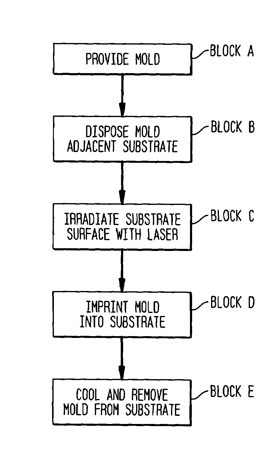
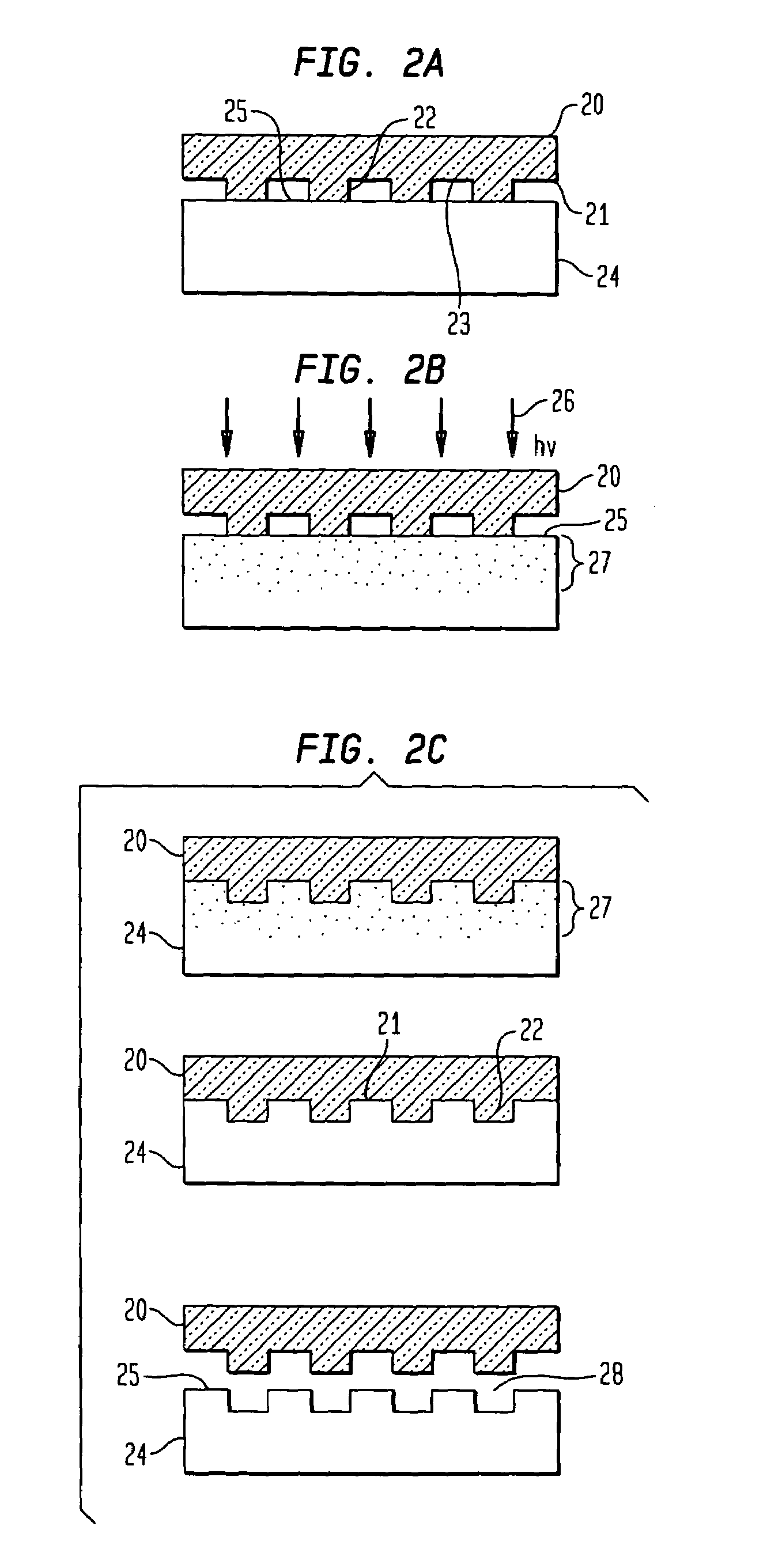
[0037]A series of experiments were conducted using molds having the following three patterns: (1) grating of 140 linewidth, 110 nm depth, and 300 nm period; (2) lines 10 nm wide and 15 nm deep, which were created due to the trenching effect in reactive ion etching during mold fabrication; and (3) rectangles of length and width in tens of microns and a depth of 110 nm. All three patterns were imprinted directly in silicon in the same LADI process.

[0038]First, a quartz mold, as described above, was brought into contact with a silicon substrate. Two large press plates were used to supply the force which pressed the mold against the substrate. The silicon wafer was placed on the lower plate with the mold on top of the wafer. The top plate, also made of fused quartz and hence transparent to the laser beam, was placed on top of the mold. The two plates were pressed together by increasing the pressure provided by screws between the two large plates. The preferred level of pressure applied ...


PUM

PropertyMeasurementUnit
Timeaaaaaaaaaa
Timeaaaaaaaaaa
Lengthaaaaaaaaaa

Abstract

In accordance with the invention, features can be directly imprinted into the surface of a solid substrate. Specifically, a substrate is directly imprinted with a desired pattern by the steps of providing a mold having a molding surface to imprint the pattern, disposing the molding surface adjacent or against the substrate surface to be imprinted, and irradiating the substrate surface with radiation to soften or liquefy the surface. The molding surface is pressed into the softened or liquefied surface to directly imprint the substrate. The substrate can be any one of a wide variety of solid materials such as semiconductors, metals, or polymers. In a preferred embodiment the substrate is silicon, the laser is a UV laser, and the mold is transparent to the UV radiation to permit irradiation of the silicon workpiece through the transparent mold. Using this method, applicants have directly imprinted into silicon large area patterns with sub-10 nanometer resolution in sub-250 nanosecond processing time. The method can also be used with a flat molding surface to planarize the substrate.

Description

CROSS REFERENCE TO RELATED APPLICATIONS[0001]This application claims the benefit of U.S. Provisional Patent Application No. 60 / 364,653 filed by Stephen Chou on Mar. 15, 2002 and entitled “A Method for Direct Imprint of Microstructures in Materials”.[0002]This application is also a continuation-in-part of U.S. patent application Ser. No. 10 / 244,276 filed by Stephen Chou on Sep. 16, 2002 and entitled “Lithographic Method For Molding Pattern With Nanoscale Features” which, in turn, is a continuation of U.S. application Ser. No. 10 / 046,594 filed by Stephen Chou on Oct. 29, 2001, which claims priority to U.S. patent application Ser. No. 09 / 107,006 filed by Stephen Chou on Jun. 30, 1998 (now U.S. Pat. No. 6,309,580 issued Oct. 30, 2001) and which, in turn, claims priority to U.S. application Ser. No. 08 / 558,809 filed by Stephen Chou on Nov. 15, 1995 (now U.S. Pat. No. 5,772,905 issued Jun. 30, 1998). All of the foregoing Related Applications are incorporated herein by reference.[0003]This...

Claims


Application Information

Patent Timeline
IPC IPC(8): B29C59/16B29C33/40B29C35/08B29C59/02
CPCB29C33/38B29C33/424B29C59/022B82Y40/00G03F7/0002B82Y10/00B29C35/0888B29C2035/0822B29C2035/0838B29C2059/023B29C2035/0827
Inventor CHOU, STEPHEN Y.
Owner PRINCETON UNIV
Why Eureka
Try Eureka