Silicided body contact SOI device

a contact device and body technology, applied in the direction of semiconductor devices, basic electric elements, electrical equipment, etc., can solve the problem that the effect of source-body-tie structure may not be sufficiently achieved, and achieve the effect of a simple process

Inactive Publication Date: 2007-05-01
SEIKO EPSON CORP
View PDF9 Cites 2 Cited by
  • Summary
  • Abstract
  • Description
  • Claims
  • Application Information

AI Technical Summary

Benefits of technology

[0010]In the semiconductor device of the present invention, the body region and the body contact region are connected through a Schottky junction. Accordingly, when a MOS transistor is operated, holes generated by the impact ionization phenomenon do not travel to a contact section, but can be directly absorbed by the body contact region. As a result, there is provided a semiconductor device having excellent characteristics in which holes generated in the body region can be excellently absorbed, and the substrate floating effect is reduced even when a high voltage is applied.
[0012]In the semiconductor device in accordance with the present invention, the body contact region can be formed of a silicide compound. According to this embodiment, a semiconductor device having a body contact region formed by a simpler process can be provided.

Problems solved by technology

In other words, holes generated by impact ionization are absorbed after moving a long distance, and therefore the effects of a source-body-tie structure may not be sufficiently attained under the recent demands for high-speed switching characteristics.

Method used


Image

  • Silicided body contact SOI device
  • Silicided body contact SOI device
  • Silicided body contact SOI device

Examples


modification example

[0056

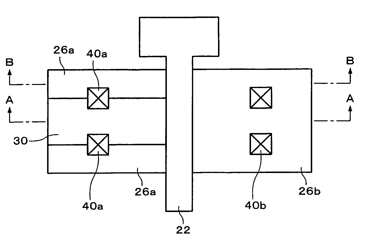
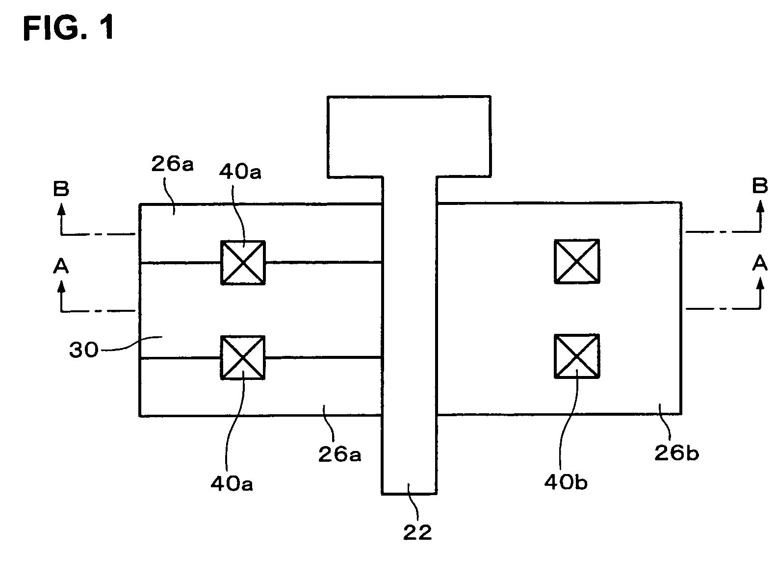
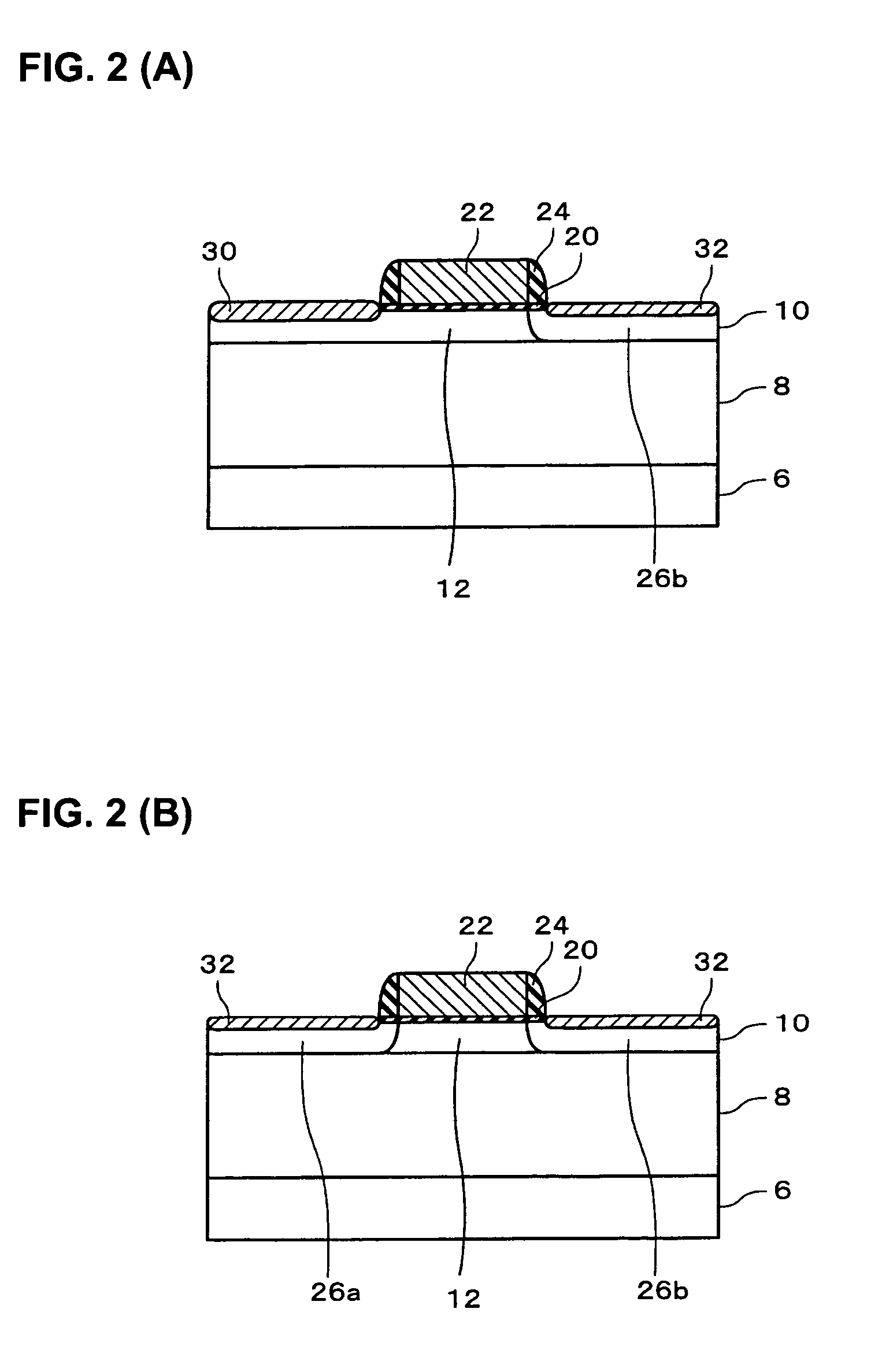
[0057]The present invention is not limited to the above-described embodiment, and can be modified within the scope of the subject matter of the present invention. As a modification example, for example, a semiconductor device shown in FIGS. 12–14 can be enumerated. FIG. 12 is a cross-sectional view schematically showing a semiconductor device in accordance with a first modification example. FIG. 13 is a cross-sectional view schematically showing a semiconductor device in accordance with a second modification example. FIG. 14 is a plan view schematically showing a semiconductor device in accordance with a third modification example. It is noted that the cross-sectional views in FIGS. 12 and 13 indicate the same sections as those shown in the cross-sectional view of FIG. 2(A).

[0058]As shown in FIG. 12, the semiconductor device in accordance with the first modification example can be provided with an LDD (lightly doped drain) region 28 between a drain region 26b and a channel regi...


PUM


Abstract

A semiconductor device includes a dielectric layer, a semiconductor layer provided above the dielectric layer, a gate dielectric layer provided above the semiconductor layer, a gate electrode provided above the gate dielectric layer, a source region and a drain region provided in the semiconductor layer, a body region other than the source region and the drain region in the semiconductor layer, and a body contact region that divides the source region in a plurality of areas and joins to the body region, wherein the body contact region is formed of a compound of a semiconductor of the semiconductor layer and a metal.

Description

RELATED APPLICATIONS[0001]This application claims priority to Japanese Patent Application No. 2004-082544 filed Mar. 22, 2004 which is hereby expressly incorporated by reference herein in its entirety.BACKGROUND[0002]1. Technical Field[0003]The present invention relates to semiconductor devices having a so-called source-body-tie structure in which a body region and a source region are connected to each other, and methods for manufacturing the same.[0004]2. Related Art[0005]Research and development are being made in recent years on insulated gate type transistors which are provided in a semiconductor layer (SOI layer: Silicon On Insulator layer) provided on a dielectric layer as devices that can realize lower power consumption and high-speed operation, compared to the case where transistors are formed in a semiconductor layer in a bulk state. Among insulated gate type field effect transistors provided in such a SOI layer, there are those having a source-body-tie structure in which a ...

Claims


Application Information

Patent Timeline
Patent Type & Authority Patents(United States)
IPC IPC(8): H01L27/12H01L21/336H01L21/74H01L27/10H01L29/417H01L29/78
CPCH01L21/743H01L29/41758H01L29/66659H01L29/7835
Inventor TAKIZAWA, TERUO
Owner SEIKO EPSON CORP
Why Eureka
Try Eureka