Method of manufacturing semiconductor device, semiconductor device, circuit substrate and electronic apparatus

a semiconductor and circuit substrate technology, applied in the direction of semiconductor/solid-state device details, antenna details, semiconductor/solid-state device details, etc., can solve the problems of conduction failure between electrodes, high density semiconductor chip packaging, and extremely restricted packaging space for semiconductor chips in the aforementioned electronic apparatuses, so as to prevent the electrodes of the semiconductor device from becoming oxidized and the effect of wettability deteriorating

Active Publication Date: 2007-05-08
SAMSUNG ELECTRONICS CO LTD
View PDF21 Cites 115 Cited by
  • Summary
  • Abstract
  • Description
  • Claims
  • Application Information

AI Technical Summary

Benefits of technology

[0014]According to this aspect, while exposing the distal end portion of the electrode at the rear surface of the semiconductor substrate, it is possible to form the second insulating layer at the periphery thereof. As a result, even if the bonded members between the electrodes are deformed when the semiconductor devices are stacked, it is possible to prevent short-circuiting between the bonded members and the rear surface of the semiconductor substrate. Accordingly, short-circuiting between the signal wiring and the ground can be prevented.
[0050]According to this aspect, even if the solder or brazing material is deformed when a plurality of the semiconductor chips are stacked, it is possible to prevent short-circuiting between the solder or brazing material and the rear surface of the semiconductor substrate. Accordingly, short-circuiting between the signal wiring and the ground can be prevented.

Problems solved by technology

Accompanying this, packaging space for semiconductor chips in the aforementioned electronic apparatuses is extremely restricted, and high density semiconductor chip packaging is a problem.
In addition, if the semiconductor chip 202a is stacked with the electrode 234 in an oxidized state, it is difficult for solder alloy to be formed in the bond portion between the solder layer 240 and the electrode 234, thereby creating the problem of conduction failures occurring between electrodes.
This results in there being a reduced yield of three-dimensionally packaged semiconductor devices.

Method used


Image

  • Method of manufacturing semiconductor device, semiconductor device, circuit substrate and electronic apparatus
  • Method of manufacturing semiconductor device, semiconductor device, circuit substrate and electronic apparatus
  • Method of manufacturing semiconductor device, semiconductor device, circuit substrate and electronic apparatus

Examples


first embodiment

(First Embodiment)

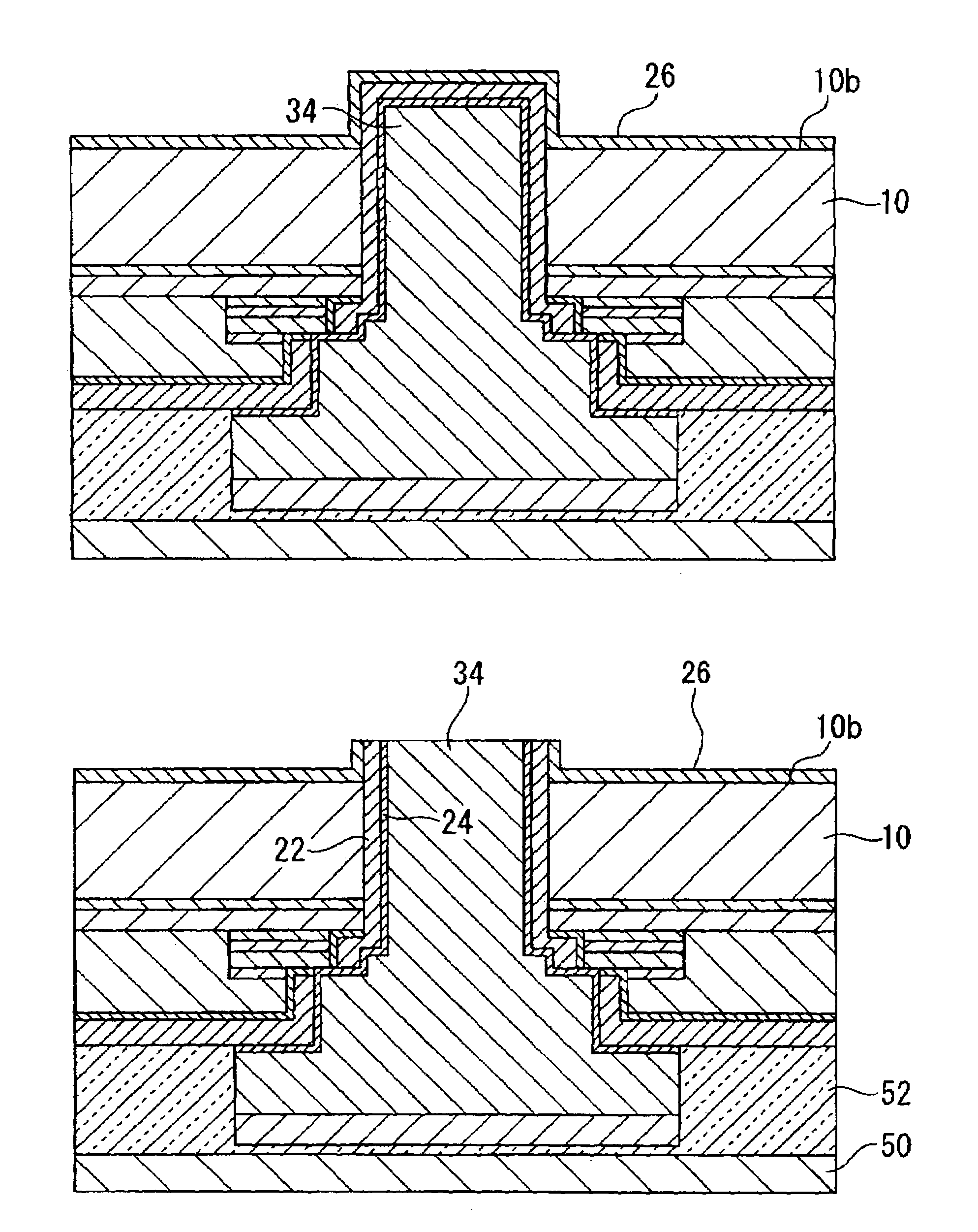
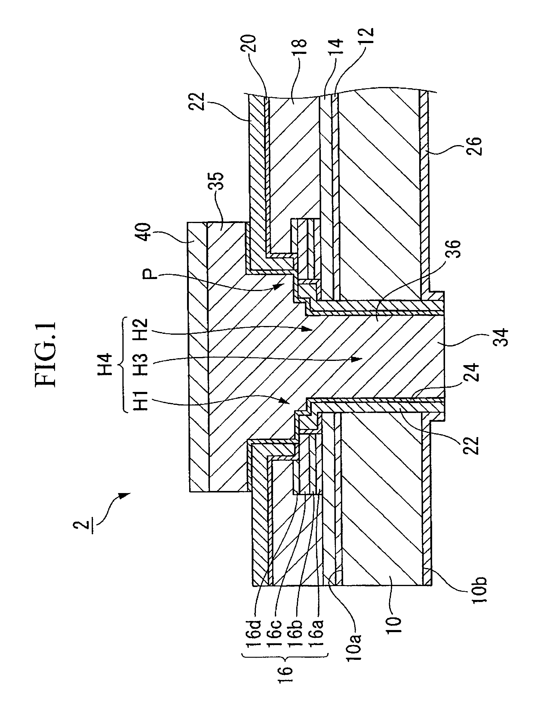
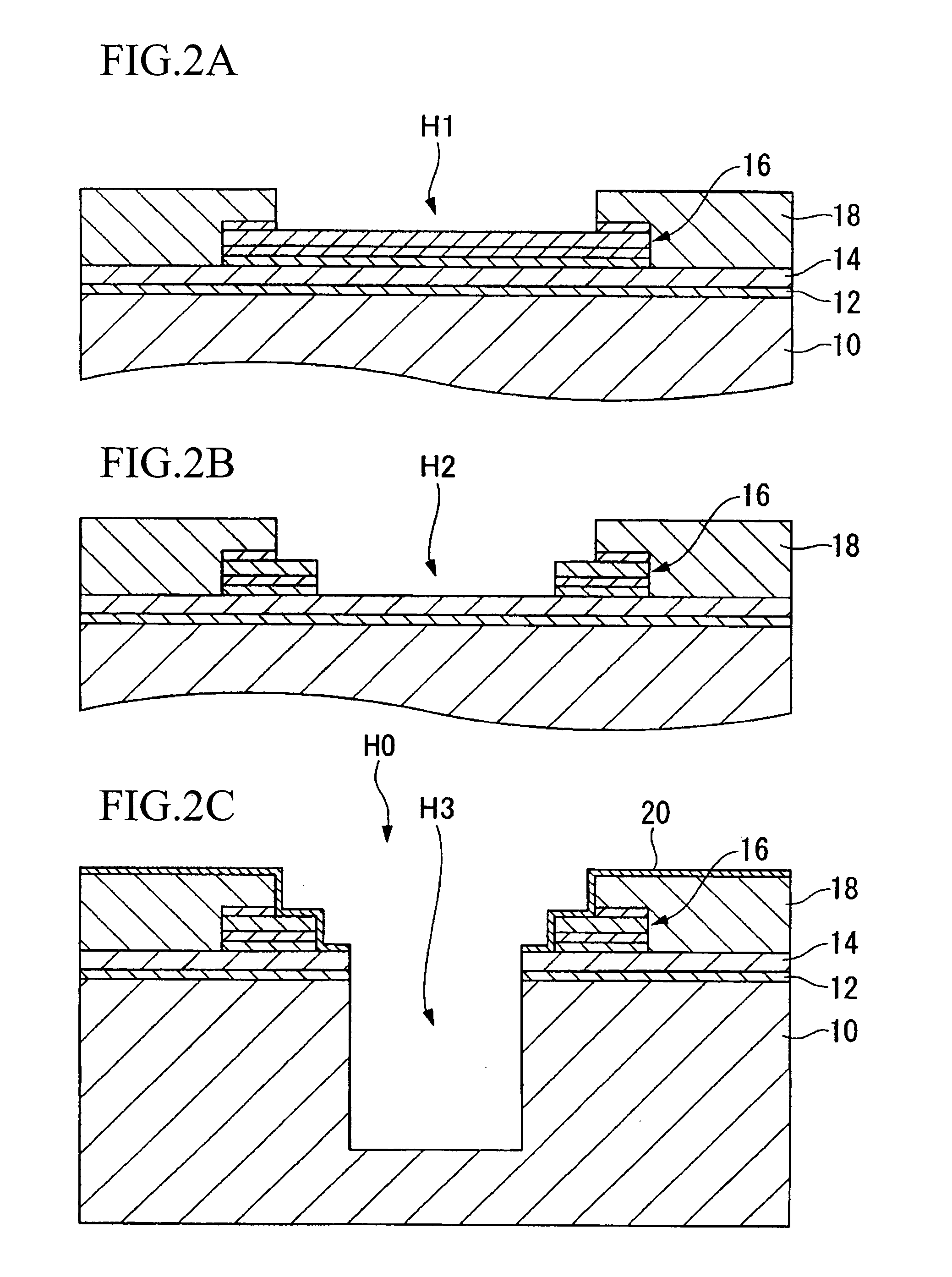
[0078]Firstly, a semiconductor chip that is the first embodiment of the semiconductor device according to the present invention will be described using FIG. 1.

[0079]FIG. 1 is a side cross-sectional view of electrode portions of a semiconductor chip according to the present embodiment.

[0080]The semiconductor chip 2 according to the present embodiment has a semiconductor substrate 10 on which an integrated circuit is formed, an electrode 34 that is formed via an insulating film 22, which is a first insulating layer, inside a through hole H4 that extends from an active surface 10a of the semiconductor substrate 10 to a rear surface 10b of the semiconductor substrate 10, and an insulating film 26, which is a second insulating layer, formed on the rear surface 10b of the substrate 10.

(Semiconductor Device)

[0081]In the semiconductor chip 2 shown in FIG. 1, an integrated circuit (not shown) formed by a transistor, memory device, or some other electronic device is formed o...

second embodiment

(Second Embodiment)

[0132]Next, the semiconductor chip according to the second embodiment of the semiconductor device of the present invention, will be described using FIG. 11.

[0133]FIG. 11 is a side cross-sectional view of electrode portions of a semiconductor chip according to the present embodiment. The semiconductor chip 3 according to the second embodiment differs from the semiconductor chip 1 of the first embodiment only in that the distal end portion of the electrode 34 on the rear side of the semiconductor chip 3 is formed on substantially the same plane as the surface of the insulating film 26, which is the second layer. The remainder of the structure is the same as that of the first embodiment and a detailed description thereof is omitted here.

[0134]In the semiconductor chip 3 of the second embodiment, the bottom end surface of the plug portion 36a of the electrode 34 is formed on substantially the same plane as the surface of the insulating film 26 formed on the rear surfa...

third embodiment

(Third Embodiment)

[0138]Next, the semiconductor chip according to the third embodiment of the semiconductor device of the present invention will be described using FIG. 12.

[0139]FIG. 12 is a side cross-sectional view showing an electrode portion of a semiconductor chip according to the present embodiment. In FIG. 12, component elements that are the same as those in FIG. 1 are given the same descriptive symbols and a description thereof is omitted.

[0140]In the semiconductor device according to the present embodiment, the basic structure is the same as that of the first embodiment shown in FIG. 1, however, the semiconductor chip 100 according to the present embodiment has an electrode body 37 that is formed via the insulating film 22, which is the first insulating film, inside the through hole H4 that is formed extending from the active surface 10a of the semiconductor substrate 10 to the rear surface 10b of the semiconductor substrate 10. The semiconductor chip 100 also has an electr...


PUM


Abstract

A method of manufacturing a semiconductor device having electrodes penetrating a semiconductor substrate, the method includes the steps of forming a concave portion extending from an active surface of a semiconductor substrate on which an integrated circuit is formed to an interior of the semiconductor substrate, forming a first insulating layer on an inner surface of the concave portion, filling an inner side of the first insulating layer with an electroconductive material so as to form an electrode, exposing a distal end portion of the first insulating layer by etching a rear surface of the semiconductor substrate, forming a second insulating layer on a rear surface of the substrate, and exposing the distal end portion of the electrode by removing the first insulating layer and the second insulating layer from a distal end portion of the electrode.

Description

BACKGROUND OF THE INVENTION[0001]1. Field of the Invention[0002]The present invention relates to a method of manufacturing a semiconductor, a semiconductor, a circuit substrate and an electronic apparatus and, in particular, to a semiconductor chip suitable for three-dimensional packaging and to a method of manufacturing the same.[0003]Priority is claimed on Japanese Patent Applications No. 2003-72337, filed Mar. 17, 2003, and No. 2003-76111, filed Mar. 19, 2003, the content of which is incorporated herein by reference.[0004]2. Description of Related Art[0005]Reductions in size and weight are demanded in portable electronic apparatuses such as mobile telephones, notebook computers, and personal digital assistance (PDA).[0006]Accompanying this, packaging space for semiconductor chips in the aforementioned electronic apparatuses is extremely restricted, and high density semiconductor chip packaging is a problem. Therefore, three-dimensional packaging technology such as that shown in, ...

Claims


Application Information

Patent Timeline
Patent Type & Authority Patents(United States)
IPC IPC(8): H01L21/44H01L21/768H01L23/12H01L23/48H01L25/065
CPCH01L21/76898H01L23/481H01L25/0657H01L25/50H01L2224/16145H01L2924/01068H01L2225/06527H01L2225/06541H01L2225/06593H01L2924/01067H01L2225/06513H01L2224/05573H01L2224/13025H01L2224/13009H01L24/03H01L24/05H01L24/11H01L24/13H01L24/16H01L2224/05639H01L2924/00014H01L2224/05644H01L2224/05664H01L2224/05669H04M1/22H01Q1/242H04N23/56
Inventor MIYAZAWA, IKUYA
Owner SAMSUNG ELECTRONICS CO LTD
Why Eureka
Try Eureka