Ink jet recording head and ink jet printer with piezoelectric element

a technology of piezoelectric element and recording head, which is applied in the field of piezoelectric element printing and ink jet recording head, can solve the problems of deterioration of the environment, failure to manufacture, and the piezoelectric element made of this material must be reconsidered, so as to achieve the effect of large electromechanical coupling coefficient, improved piezoelectric characteristics, and high performan

Active Publication Date: 2007-05-15
SEIKO EPSON CORP
View PDF2 Cites 30 Cited by
  • Summary
  • Abstract
  • Description
  • Claims
  • Application Information

AI Technical Summary

Benefits of technology

[0011]In view of these circumstances, the object of the present invention is to provide a piezoelectric element which has a high performance and does not include Pb, and is formed by thin film processes including the direct implementation on a Si substrate, and an ink jet recording head, an ink jet printer, a surface acoustic wave element, a frequency-dependent filter, an oscillator, an electronic circuit, a thin film piezoelectric resonator and an electronic apparatus, in which the piezoelectric element is used.
[0057]According to the electronic apparatus, the piezoelectric material film has better piezoelectric characteristics, and therefore, this piezoelectric material film has a large electromechanical coupling coefficient, and thereby miniaturization with high performance can be realized.

Problems solved by technology

In addition, especially regarding the piezoelectric element made of PZT, since it includes Pb as a constituent and the evaporation of Pb leads to deterioration of the environment because Pb is harmful, manufacturing the piezoelectric element made of this material must reconsidered.
In the case in which an attempt is made to manufacture a piezoelectric element used in the recording head for the ink jet printer using a piezoelectric material film of this BiFeO3, there is a problem in that the manufacture is not successful because it is very difficult to directly use BiFeO3 on a Si substrate.
This is because a natural oxide film normally forms on the Si substrate, and it is difficult to make a BiFeO3 film grow epitaxially on the natural oxide film, and, for this reason, a piezoelectric material film made of BiFeO3 cannot be formed on the Si substrate.

Method used


Image

  • Ink jet recording head and ink jet printer with piezoelectric element
  • Ink jet recording head and ink jet printer with piezoelectric element
  • Ink jet recording head and ink jet printer with piezoelectric element

Examples


Embodiment Construction

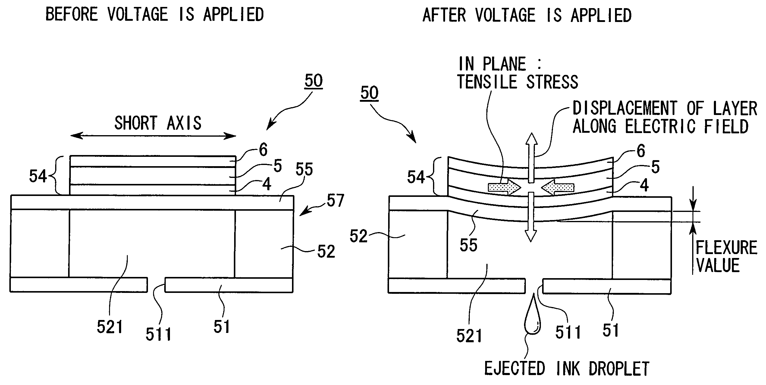
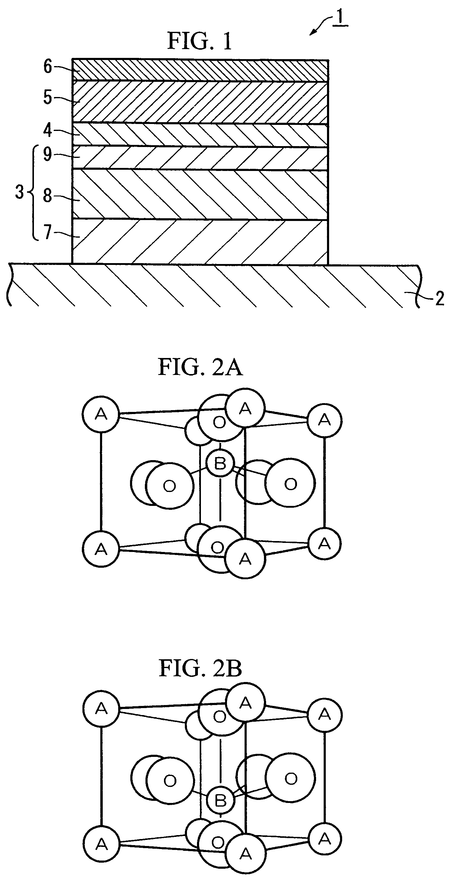
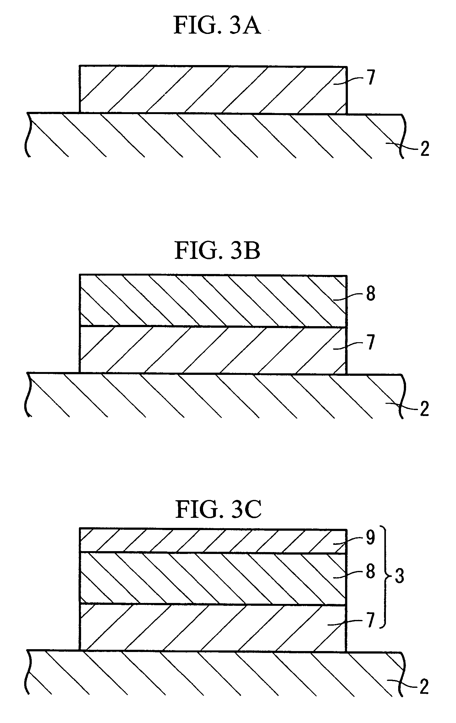
[0077]A layer formed of grains with a single orientation, i.e., only with an orientation parallel to the through-thickness of a layer, is preferably used as the buffer layer 3, and it is more preferable that the grains in the buffer layer also have a planer orientation, i.e., the grains have orientations in all three-dimensions. This is because good bonding or adhesion between a base substance 2 made of the Si substrate with a natural oxide film thereon and the lower electrode 4 described later can be attained by including the buffer layer 3.

[0078]It is preferable that this buffer layer 3 include at least one of metal oxides with a NaCl structure, metal oxides with a fluorite structure, and metal oxides with a perovskite structure, and it is especially preferable that the buffer layer 3 be formed of a layered structure of a metal oxide with a NaCl structure or a metal oxide with a fluorite structure, and a metal oxide with a perovskite structure. This is because the lattice mismatch...


PUM


Abstract

A piezoelectric element includes a piezoelectric material film made of BiFeO3. The piezoelectric element can be used in an ink jet recording head which includes a cavity with a variable internal volume, wherein the internal volume of the cavity changes depending on deformation of the piezoelectric material film included in the piezoelectric element.

Description

BACKGROUND OF THE INVENTION[0001]1. Field of the Invention[0002]This invention relates to a piezoelectric element including a BiFeO3 piezoelectric film, an ink jet recording head, an ink jet printer, a surface acoustic wave element, a frequency-dependent filter, an oscillator, an electronic circuit, a thin film piezoelectric resonator and an electronic apparatus.[0003]Priority is claimed on Japanese Patent Application No. 2003-181153, filed Jun. 25, 2003, and Japanese Patent Application No. 2003-308967, filed Sep. 1, 2003, the contents of which are incorporated herein by reference.[0004]2. Description of Related Art[0005]An ink jet printer is known as a high-resolution and high speed printing printer. The ink jet printer is provided with an ink jet recording head which comprises a cavity with a variable internal volume, and, in the ink jet printer, printing is carried out by ejecting ink droplets from nozzles while the head scans. A piezoelectric element made of ceramic as represent...

Claims


Application Information

Patent Timeline
Patent Type & Authority Patents(United States)
IPC IPC(8): B41J2/045B41J2/055B41J2/135B41J2/14H01L41/08H01L41/09H01L41/18H01L41/22H01L41/29H01L41/319H01L41/39H02N2/00H03H3/02H03H3/08H03H9/02H03H9/05H03H9/17H03H9/25
CPCB41J2/14233H03H3/02H03H9/02094H03H9/02133H03H9/0542H03H9/172H03H9/173H03H9/174H01L41/0478H01L41/1878H01L41/316H01L41/319H01L41/0815H10N30/878H10N30/10516H10N30/8561H10N30/076H10N30/079
Inventor MIYAZAWA, HIROMUHIGUCHI, TAKAMITSUIWASHITA, SETSUYA
Owner SEIKO EPSON CORP
Why Eureka
Try Eureka