Method for connecting an integrated circuit to a substrate and corresponding circuit arrangement

Inactive Publication Date: 2007-05-15
POLARIS INNOVATIONS
View PDF15 Cites 6 Cited by
  • Summary
  • Abstract
  • Description
  • Claims
  • Application Information

AI Technical Summary

Benefits of technology

[0013]An object of the present invention is to provide a more simple and low-cost method for connecting an integrated circuit to a substrate and a corresponding circuit arrangement, which method remains largely uninfluenced by thermal mismatch and ensures a reliable electrical contact.
[0018]The elastic contact structure provided according to the invention makes it possible to compensate for differences in the linear expansion in the connecting plane that exist between the elements involved, and also to achieve a reliable electrical contact between the elements involved in the direction of compression. In the case of such connections, a mechanical connection and an electrical contact can be advantageously produced in one working step.
[0028]According to a further preferred development, the adhesive layer has such an elasticity that, when there is different thermal expansion of the substrate and the integrated circuit, it makes it possible for them to be displaced with respect to each other in the common plane of the first and second main areas.

Problems solved by technology

CSP (chip size package) or WLP (wafer level package) solutions for connecting an integrated circuit to a substrate have problems with respect to reliability when there are temperature changes, in particular in the case of large chips.
In the case of this customary solution, the mismatch of the thermal properties of the chip and the substrate, in particular the coefficient of thermal expansion, leads to greater risks in terms of reliability.
In particular in the case of large chips, this limits the reliability considerably.
Further disadvantages of the known solutions are the high space requirement, the high radio-frequency impedances and also a lack of suitability for direct chip / chip or chip / substrate contact.

Method used


Image

  • Method for connecting an integrated circuit to a substrate and corresponding circuit arrangement
  • Method for connecting an integrated circuit to a substrate and corresponding circuit arrangement
  • Method for connecting an integrated circuit to a substrate and corresponding circuit arrangement

Examples


first embodiment

[0034]FIGS. 1a,b are schematic representations of a method for connecting an integrated circuit to a substrate according to the present invention.

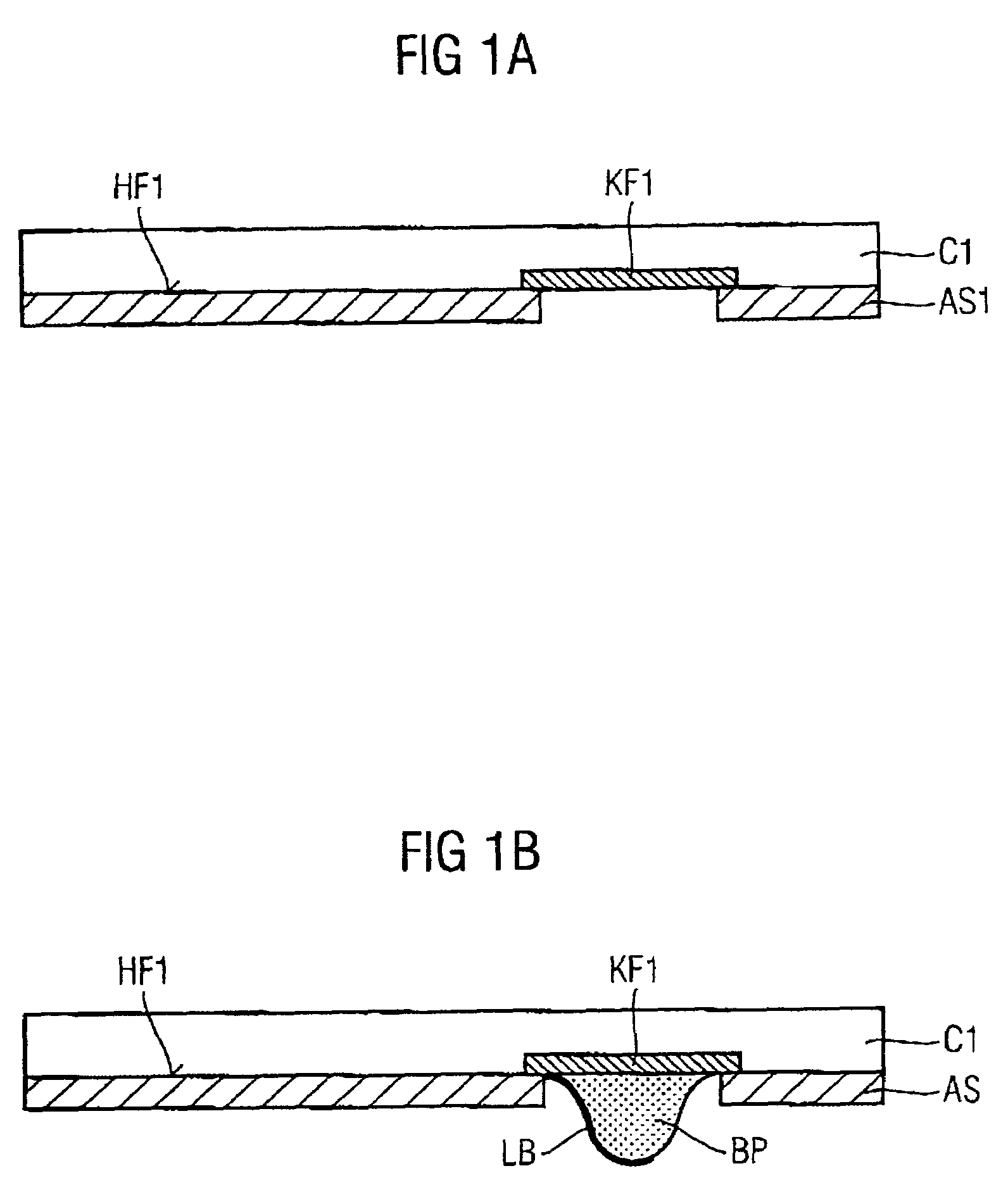
[0035]In FIG. 1a, reference numeral C1 designates a first integrated circuit in chip form, which has a first contact area KF1 in a main area HF1. The main area HF1 also has a covering layer AS1 of polyimide, which covers the main area HF1 surrounding the contact area and overlaps the periphery of the contact area KF1.

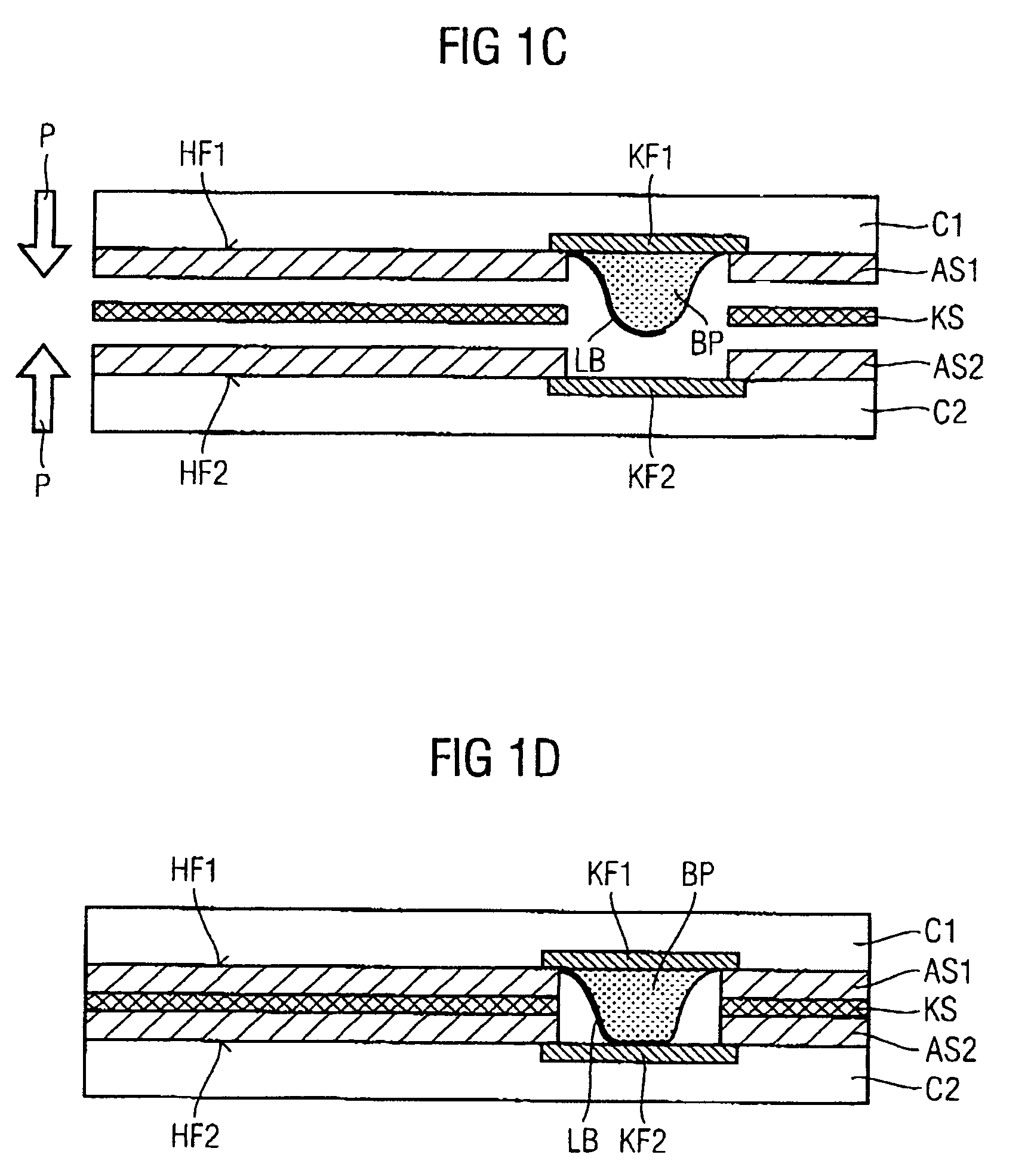
[0036]In a further method step, which is illustrated in FIG. 1b, a nonconducting elastic elevation BP is provided on the contact area KF1 and its upper side is connected to the contact area KF1 by means of an interconnect LB. Preferred technologies for producing the elastic elevation BP are printing technology, dispensing, ink-jetting, spin-coating, spraying or photolithography. In particular in the case of a nonconductive elastic elevation BP, the interconnect LB may be realized by partial metallization by means of sputtering...

second embodiment

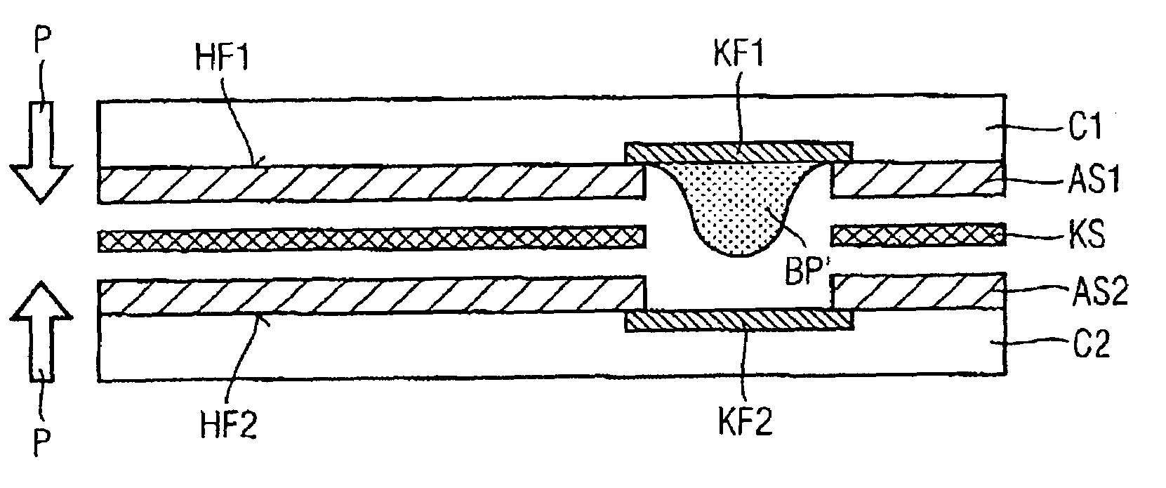
[0040]FIGS. 2a,b are schematic representations of a method for connecting an integrated circuit to a substrate according to the present invention.

[0041]The second exemplary embodiment, described in FIGS. 2a–d, differs from the first exemplary embodiment described above only in that the elastic elevation BP′ is conductive, that is to say the interconnect LB can be omitted. This conductivity is achieved for example by admixing a conductive component with the elastic plastic.

[0042]Although the present invention has been described above on the basis of a preferred exemplary embodiment, it is not restricted to this but can be modified in a wide variety of ways.

[0043]The present invention can in particular be applied not only to chips but also to hybrids, wafers or other integrated circuits.

[0044]It goes without saying that the substrate could, however, also be a printed circuit board or some other substrate. In the case of the mounting of a chip, which is produced for example from silico...


PUM


Abstract

Method for connecting an integrated circuit to a substrate and corresponding circuit arrangementThe present invention provides a method for connecting an integrated circuit (C1), in particular a chip or a wafer or a hybrid, to a substrate (C2), which has the following steps: provision of a first electrical contact structure (KF1, BP, LB; KF1, BP′) on a first main area (HF1) of the integrated circuit (C1); provision of a corresponding second electrical contact structure (KF2) on a second main area (HF2) of the substrate (C2); at least one of the contact structures, the first electrical contact structure (KF1, BP, LB; KF1, BP′) or the second electrical contact structure (KF2), being elastic; placement of the first electrical contact structure (KF1, BP, LB; KF1, BP′) onto the corresponding second electrical contact structure (KF2), so that both are in electrical contact and under mechanical compression pressure (P); and connection of a region of the main area (HF1) surrounding the first electrical contact structure (KF1, BP, LB; KF1, BP′) to a corresponding region surrounding the second electrical contact structure (KF2) of the second main area (HF2) by an adhesive layer (KS), so that the first electrical contact structure (KF1, BP, LB; KF1, BP′) and / or the second electrical contact structure (KF2) are compressed in the connected state. The invention likewise provides a corresponding circuit arrangement.

Description

CROSS-REFERENCE TO RELATED APPLICATION[0001]This application claims the benefit of Germany Patent Application No. 102004030813.6, filed Jun. 25, 2004, the contents of which are hereby incorporated herein by reference in their entirety.[0002]1. Technical Field[0003]The present invention relates to a method for connecting an integrated circuit to a substrate and relates to a corresponding circuit arrangement.[0004]2. Background Art[0005]Although it can in principle be applied to any desired integrated circuits, the present invention and the problems on which it is based are explained with respect to chips with integrated circuits in silicon technology.[0006]The classic solution for connecting an integrated circuit to a substrate provides wire bonds, which have a high space requirement.[0007]CSP (chip size package) or WLP (wafer level package) solutions for connecting an integrated circuit to a substrate have problems with respect to reliability when there are temperature changes, in p...

Claims


Application Information

Patent Timeline
IPC IPC(8): H01L21/44H01L21/60H01L21/98H01L23/31H01L23/485H01L23/498H01L25/065H01L25/16H01L27/148
CPCH01L23/3157H01L24/01H01L24/72H01L25/0657H01L25/16H01L25/50H01L24/29H01L23/49811H01L2924/07811H01L24/90H01L2224/13021H01L2224/16H01L2224/83101H01L2224/83194H01L2224/90H01L2225/06513H01L2225/06524H01L2225/06589H01L2924/01005H01L2924/01015H01L2924/01078H01L2924/01079H01L2924/01082H01L2924/14H01L2924/15311H01L2924/3011H01L2924/01006H01L2924/01072H01L2224/16111H01L24/13H01L24/16H01L24/32H01L24/81H01L24/83H01L2224/16145H01L2224/73203H01L2224/81903H01L2224/05567H01L2224/05573H01L2224/05644H01L24/05H01L2924/00012H01L2924/00014
Inventor HEDLER, HARRYMEYER, THORSTEN
Owner POLARIS INNOVATIONS
Why Eureka
Try Eureka