System and method for stress free conductor removal

a conductor and stress-free technology, applied in the direction of semiconductor devices, semiconductor/solid-state device details, electric discharge tubes, etc., can solve the problems of ecp typically having a relatively low throughput, unnecessary overburden portion of conductive material, and each process has significant shortfalls, so as to improve improve the planarity, and reduce the overall k value of the dielectric stack

Inactive Publication Date: 2007-05-15
LAM RES CORP
View PDF115 Cites 23 Cited by
  • Summary
  • Abstract
  • Description
  • Claims
  • Application Information

AI Technical Summary

Benefits of technology

[0018]The present invention provides the advantage of improved planarity, more accurate mask application. Further, the overall k value of the dielectric stack can be reduced by substantially eliminating non-low-k dielectric materials from the dielectric stack.

Problems solved by technology

The overburden portion of the conductive material is unnecessary and undesirable and must be removed both to produce a damascene feature and to provide a planar surface for subsequent processing.
Each of these processes has significant shortfalls.
By way of example, ECP typically has a relatively low throughput, poor uniformity and inability to effectively remove non-conductive material.
CMP requires physical contact processes which typically leave conductive residues, or cause corrosion of the various materials, or result in non-uniform removal, and the inability to suitably planarize interconnect and interlevel dielectric (ILD) top surface.
CMP can also cause stress related damage (e.g., interlayer delamination, peeling) to remaining interconnect and ILD structures.
The CMP-caused stress damage is further exacerbated by the very poor inter-layer adhesion characteristics of the more-recently used materials.
Reducing the physical force of the CMP process to reduce the physical stress can often result in unacceptably low throughput rates and other poor process performance parameters.
CMP can also cause excessive erosion of ILD typically varying with feature dimensions and density.

Method used


Image

  • System and method for stress free conductor removal
  • System and method for stress free conductor removal
  • System and method for stress free conductor removal

Examples


Embodiment Construction

[0044]Several exemplary embodiments for an improved planarizing system and method will now be described. It will be apparent to those skilled in the art that the present invention may be practiced without some or all of the specific details set forth herein.

[0045]One embodiment of an improved planarizing system and method provides improved local planarization uniformity across a local portion of a semiconductor substrate. The improved local planarization uniformity substantially eliminates local nonuniformities caused by features in underlying layers and variations in deposition processes. Another embodiment provides improved global planarization uniformity across the entire substrate (e.g., edge uniformity as compared to center uniformity).

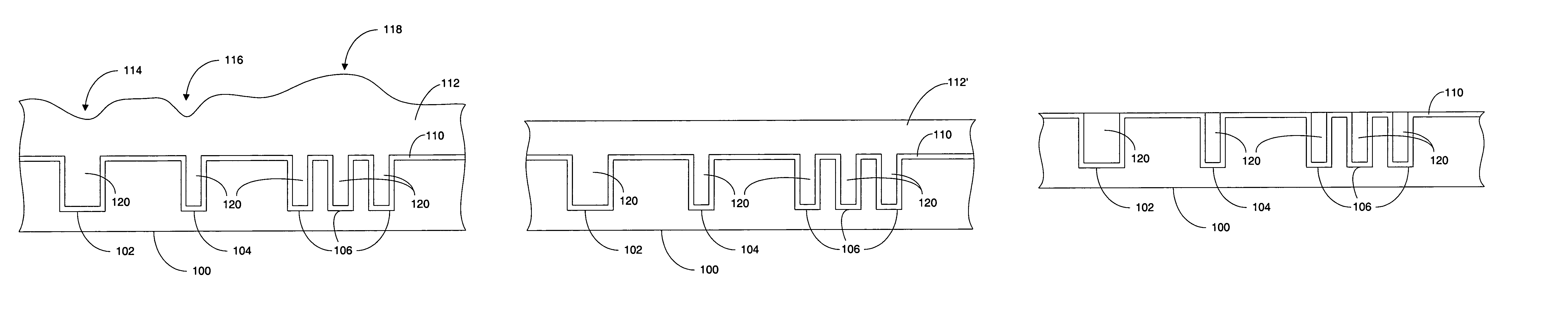
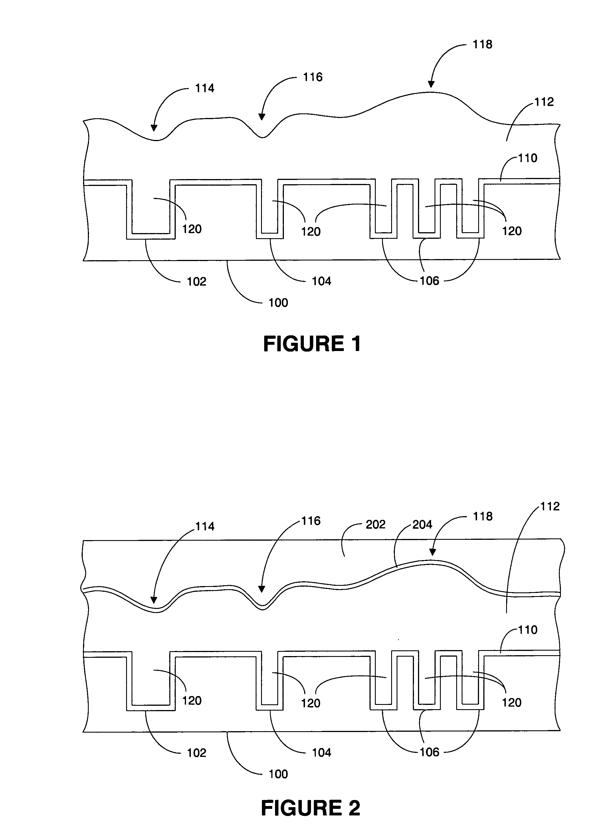
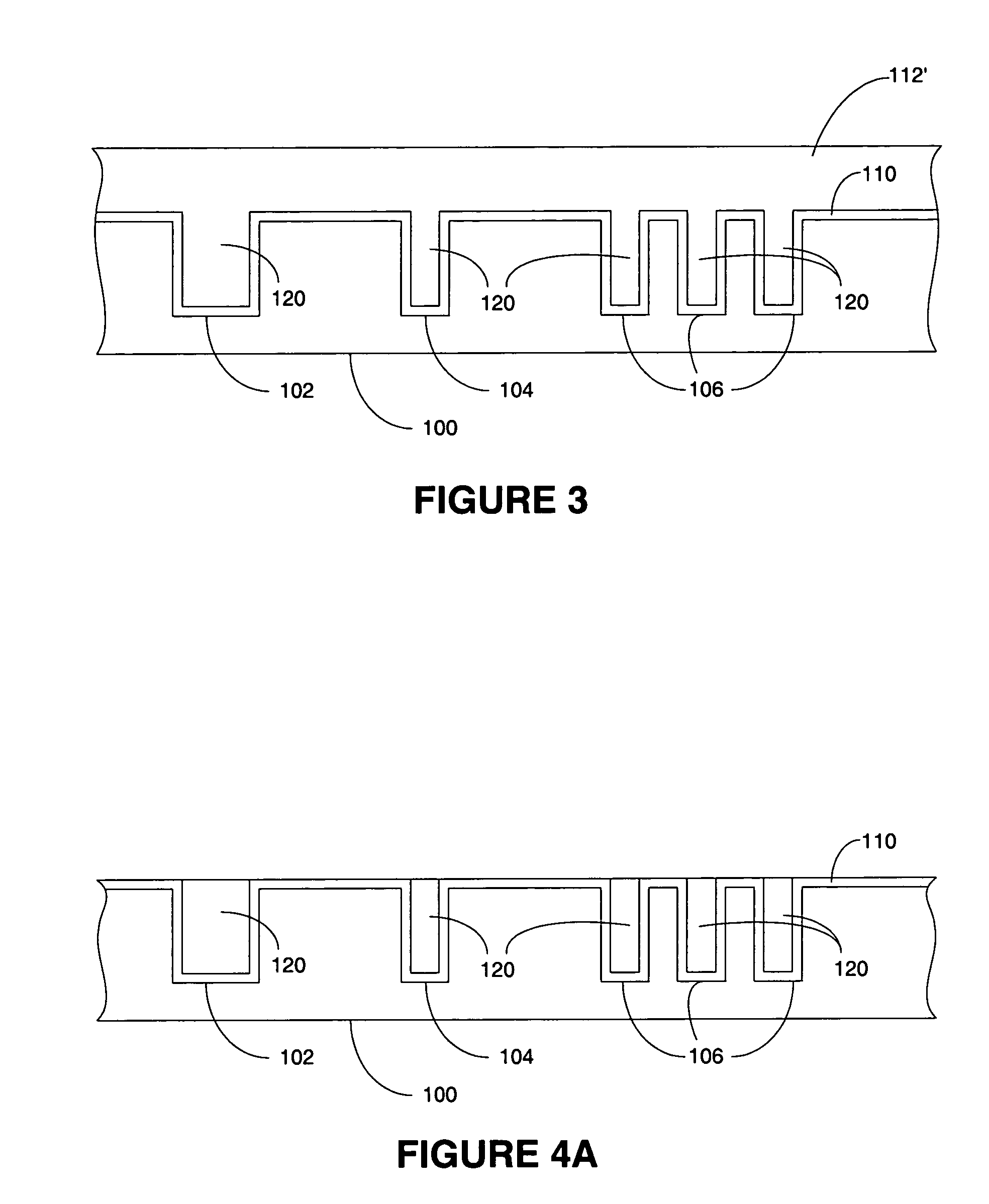
[0046]FIG. 1 shows a patterned semiconductor substrate 100 in a dual damascene process in accordance with one embodiment of the present invention. The substrate 100 has been patterned as part of the semiconductor manufacturing process such as a d...


PUM


Abstract

A system and method for forming a semiconductor in a dual damascene structure including receiving a patterned semiconductor substrate. The semiconductor substrate having a first conductive interconnect material filling multiple features in the pattern. The first conductive interconnect material having an overburden portion. The over burden portion is planarized. The over burden portion is substantially entirely removed in the planarizing process. A mask layer is reduced and a subsequent dielectric layer is formed on the planarized over burden portion. A mask is formed on the subsequent dielectric layer. One or more features are formed in the subsequent dielectric layer and the features are filled with a second conductive interconnect material.

Description

CROSS REFERENCE TO RELATED APPLICATIONS[0001]This application is a continuation-in-part of and claims priority from U.S. Pat. No. 6,939,796, application Ser. No. 10 / 390,117 filed on Mar. 14, 2003 and entitled “System, Method and Apparatus For Improved Global Dual-Damascene Planarization,” which is incorporated herein by reference in its entirety. This application is also a continuation-in-part of and claims priority from U.S. Pat. No. 6,821,899, application Ser. No. 10 / 390,520 filed on Mar. 14, 2003 and entitled “System, Method and Apparatus For Improved Local Dual-Damascene Planarization,” which is incorporated herein by reference in its entirety.BACKGROUND OF THE INVENTION[0002]1. Field of the Invention[0003]The present invention relates generally to dual damascene semiconductor manufacturing processes, and more particularly, to methods and systems for planarizing features and layers in a semiconductor manufacturing process.[0004]2. Description of the Related Art[0005]Single and d...

Claims


Application Information

Patent Timeline
Patent Type & Authority Patents(United States)
IPC IPC(8): H01L21/4763H01J37/32H01L21/00H01L21/302H01L21/311H01L21/321H01L21/3213H01L21/44H01L21/461H01L21/768H01L23/48H01L23/52H01L29/24H01L29/40H01L33/00
CPCH01J37/32522H01L21/31116H01L21/32115H01L21/32135H01L21/32136H01L21/67034H01L21/67051H01L21/6708H01L21/76819H01L21/7684H01J2237/022H01L21/28H01L21/768
Inventor BAILEY, III, ANDREW D.LOHOKARE, SHRIKANT P.
Owner LAM RES CORP
Why Eureka
Try Eureka