Arithmetic circuit integrated with a variable resistance memory element

a memory element and variable resistance technology, applied in the field of arithmetic circuits, can solve the problems of low writing voltage and complicated peripheral circuits, and achieve the effect of controlling power consumption

Inactive Publication Date: 2007-05-22
SONY CORP
View PDF6 Cites 30 Cited by
  • Summary
  • Abstract
  • Description
  • Claims
  • Application Information

AI Technical Summary

Benefits of technology

[0089]The present invention addresses the above-identified, and other problems associated with conventional methods and apparatuses and provides the arithmetic circuit in which a circuit such as a logic-in-memory that is small and operates at high speed is obtained, various operations can be performed, and high versatility can be obtained.
[0100]Further, the period of time when the intermediate state exists is short and, other than that time, since one of two variable resistance elements is in the state of high resistance, the composite resistance of the whole of the memory element becomes high to be constant, and the electric current flowing through the memory element becomes small. In this way, on the occasions of data recording or erasing and data read-out, the flowing electric current by applying the voltage to the memory element can be reduced.
[0108]Further, because the value of voltage of the output terminal can be made binary, only one kind of a threshold voltage for the output is needed; therefore the configuration of next stage of the arithmetic circuit can be simplified.
[0110]Furthermore, because the composite resistance in the stable state is high and constant, the electric current that flows through the variable resistance element becomes small and the power consumption can be controlled.

Problems solved by technology

However, there are some problems in the case of constituting the logic-in-memory with using the above-described three kinds of non-volatile devices.
First, in comparison with the floating gate MOS transistor, the writing voltage becomes low, however, is still larger than the power voltage for a typical CMOS circuit; therefore another power source or the power booster circuit is required.
Secondly, in order to change the AND operation and the OR operation, the gate voltage has three values due to the offset given to the external input data, and therefore, the peripheral circuit becomes complicated.

Method used


Image

  • Arithmetic circuit integrated with a variable resistance memory element
  • Arithmetic circuit integrated with a variable resistance memory element
  • Arithmetic circuit integrated with a variable resistance memory element

Examples


Embodiment Construction

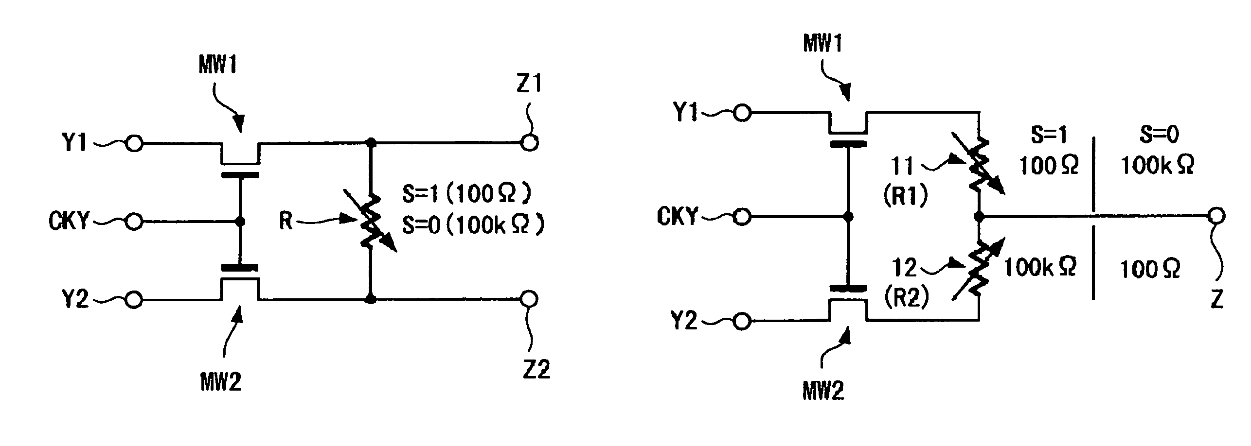
[0120]As an embodiment of the arithmetic circuit of the present invention, a schematic configuration diagram (circuit diagram) is shown in FIG. 1.

[0121]This arithmetic circuit constitutes the logic-in-memory mentioned above, and includes one non-volatile device and four MOS transistors for the control use.

[0122]In the arithmetic circuit according to an embodiment of the present invention, a variable resistance element R is specifically used as the non-volatile device instead of the various non-volatile devices described above (such as a ferroelectric, ferroelectric capacitor and TMR element).

[0123]In a variable resistance element R, a terminal Z1 and a terminal Z2 are provided at both ends.

[0124]In a MOS transistor MRD, a source is connected to the terminal Z1, and a drain is connected to an external input X, and a terminal of clock CKX is connected to a gate.

[0125]In a MOS transistor MRS, a source is connected to the terminal Z2, and a drain is connected to an external input W, and...


PUM


Abstract

An arithmetic circuit is provided having a compact and high-speed logic-in-memory wherein various operations are performed. The arithmetic circuit includes a memory element having a variable resistance element R in which the state of resistance changes reversibly between the state of high resistance and the state of low resistance by applying voltages with different polarities between one electrode and the other electrode, and at least one transistor of MRD, MRS, MW1 and MW2 connected respectively to both ends of the memory element; wherein data is stored in the memory element, the operation for the external data X, W, Y1 and Y2 input through any of the transistors is performed by applying potential to each of the ends of the memory element through the transistors MRD, MRS, MW1, and MW2, and a result of the operation is output from the memory element.

Description

CROSS REFERENCES TO RELATED APPLICATIONS[0001]The present invention contains subject matter related to Japanese Patent Application JP 2004-226970 filed in the Japanese Patent Office on Aug. 3, 2004, the entire contents of which being incorporated herein by reference.BACKGROUND OF THE INVENTION[0002]1. Field of the Invention[0003]The present invention relates to an arithmetic circuit in which an arithmetic unit and a memory are integrated.[0004]2. Description of the Related Art[0005]The configuration called logic-in-memory has been studied to obtain a circuit in which no information is lost even if the power is turned off and to obtain a circuit in which data transfer to separate RAM chips is not required, by constituting a logic circuit with a non-volatile device.[0006]For example, a floating gate type MOS transistor, ferroelectric device, TMR device and the like are proposed as the non-volatile device used in the logic-in-memory (refer to Non-patent literatures 1 to 4, for example)...

Claims


Application Information

Patent Timeline
Patent Type & Authority Patents(United States)
IPC IPC(8): G11C11/21H03K19/20
CPCG11C11/22G11C13/02G11C15/046G11C11/223G11C13/0004
Inventor HARA, MASAAKIOKAZAKI, NOBUMICHI
Owner SONY CORP
Why Eureka
Try Eureka