Semiconductor device and method for fabricating the same

a semiconductor device and capacitor technology, applied in the direction of transistors, solid-state devices, capacitors, etc., can solve the problems of capacitors not having the capacitors being manufactured as semiconductor devices, etc., and achieve the effect of desired capacitance with stability

Active Publication Date: 2007-05-29
GK BRIDGE 1
View PDF3 Cites 15 Cited by
  • Summary
  • Abstract
  • Description
  • Claims
  • Application Information

AI Technical Summary

Benefits of technology

[0018]An object of the present invention is to allow capacitors each having a lower electrode of a concave shape in cross section to have a desired capacitance with stability.
[0021]According to the semiconductor device of the present invention, the end of the second insulating film located on the sides of the opening is formed in an eaves-like part to project like eaves inwardly beyond the sides of the cavity of the first insulating film. Therefore, the side parts of the lower electrode of a concave shape in cross section formed on the bottom and sides of the cavity of the first insulating film are located under the eaves-like part of the second insulating film. This prevents the top ends of the side parts of the lower electrode of a concave shape in cross section from being etched even if a film for the formation of the lower electrode is over-etched during the formation of the lower electrode. As a result, the surface area of the lower electrode has a fixed value. Furthermore, the surface areas of lower electrodes on the semiconductor substrate do not vary. Thus, capacitors can have a desired capacitance with stability.
[0025]In the semiconductor device of the present invention, it is preferable that the lower electrode is made of a doped polysilicon film and roughened polysilicon is formed on the surface of the lower electrode. Thus, this roughened polysilicon increases the surface area of the lower electrode, resulting in the increased capacitance of a capacitor.
[0028]According to the method of the present invention, the eaves-like part is formed in the second insulating film formed on the first insulating film. Therefore, the top ends of the side parts of the lower electrode of a concave shape in cross section is not etched even during the overetching of the conductive film for a lower electrode for the formation of the lower electrode. As a result, the surface area of the lower electrode has a fixed value. Furthermore, the surface areas of lower electrodes on the semiconductor substrate do not vary. Thus, capacitors can have a desired capacitance with stability.

Problems solved by technology

However, the known method for fabricating a capacitor, i.e., a semiconductor device, has the following problems.
As a result, capacitors cannot have a desired capacitance with stability.

Method used


Image

  • Semiconductor device and method for fabricating the same
  • Semiconductor device and method for fabricating the same
  • Semiconductor device and method for fabricating the same

Examples


Embodiment Construction

[0040]An embodiment of the present invention will be described hereinafter with reference to the drawings.

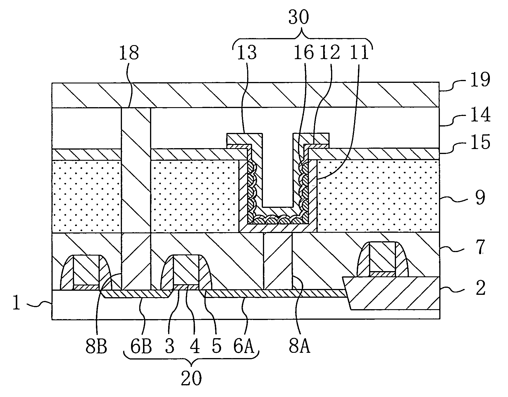
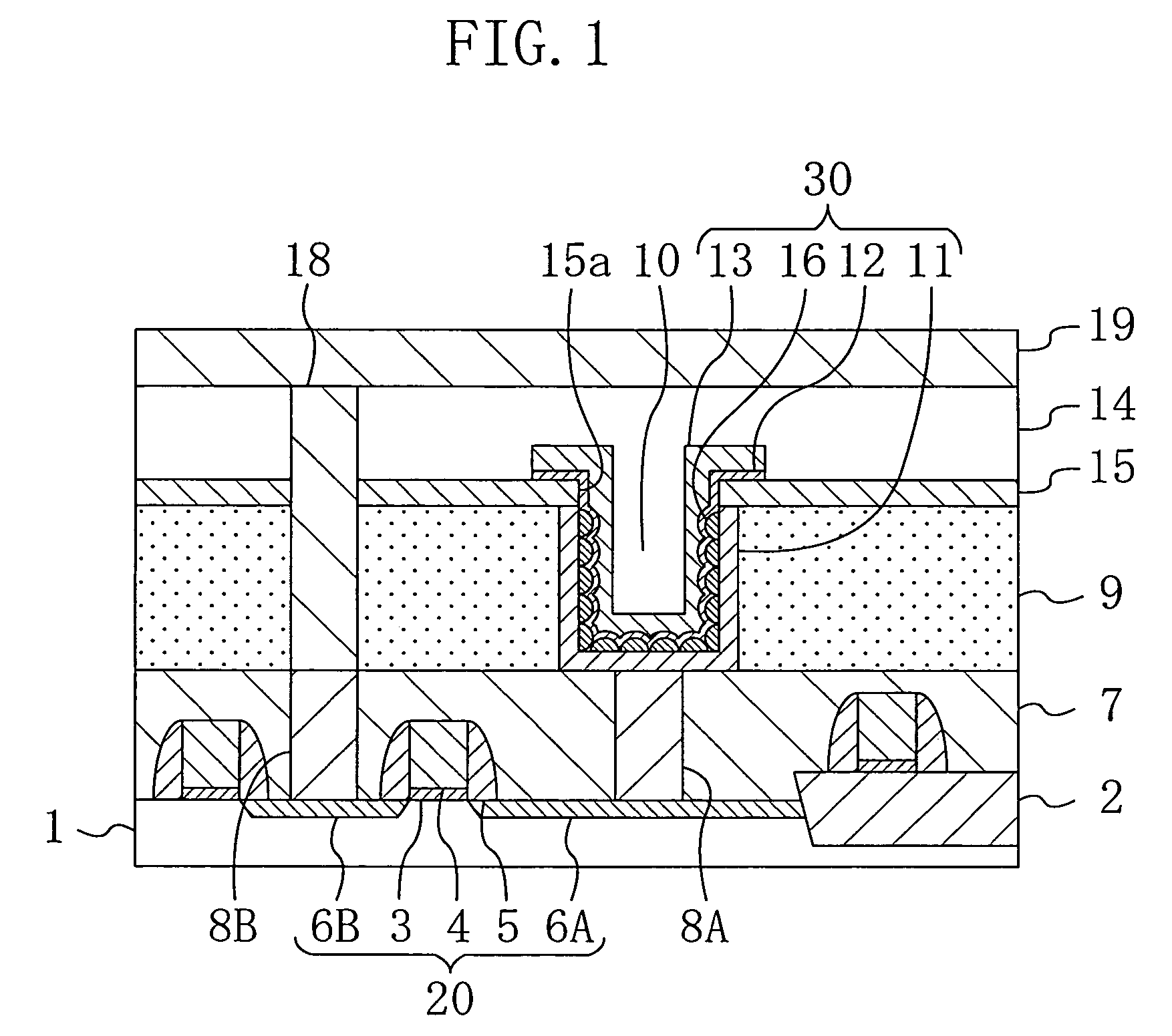
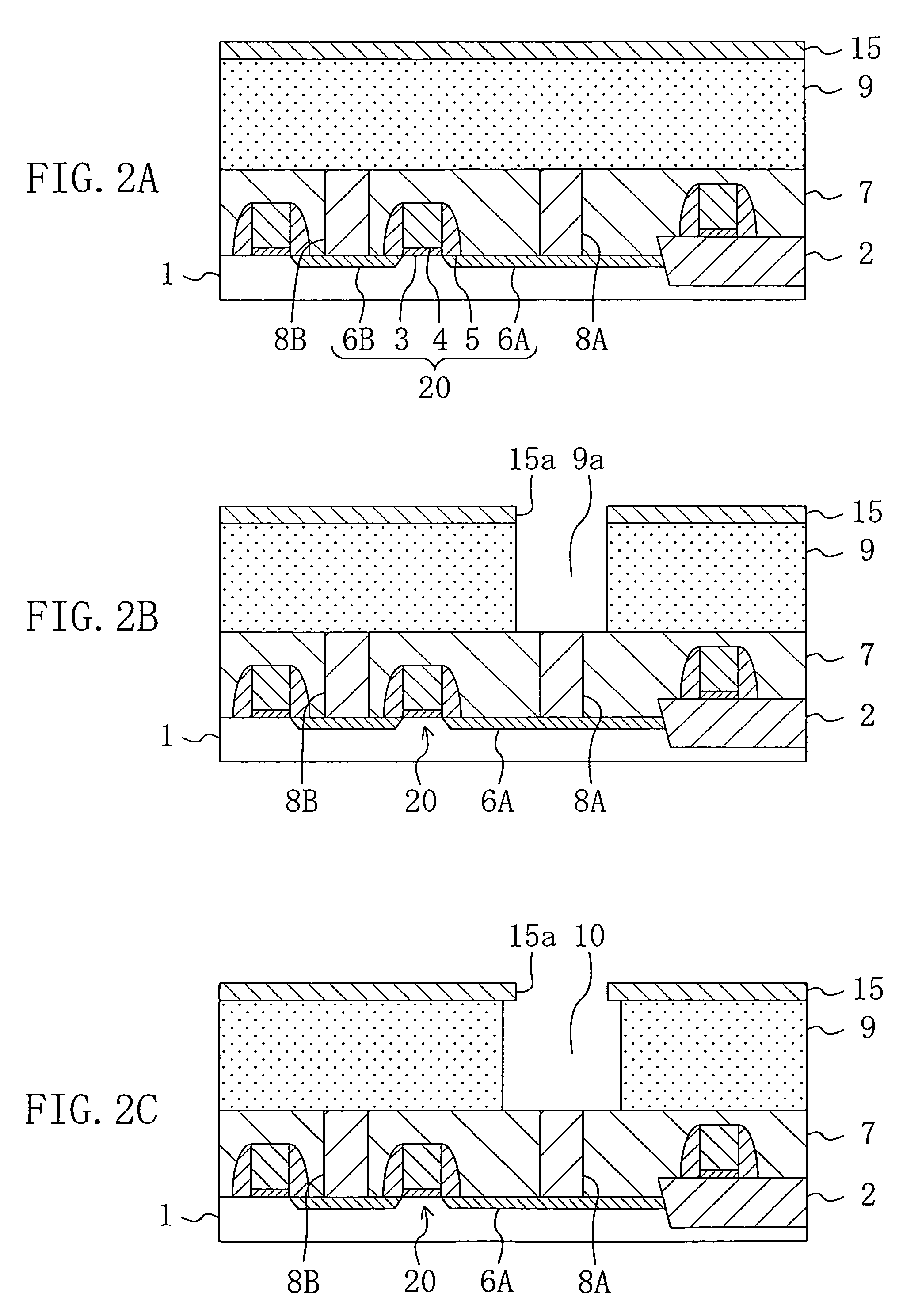
[0041]FIG. 1 shows the cross-sectional structure of a semiconductor device according to an embodiment of the present invention. As shown in FIG. 1, a semiconductor device comprises a shallow trench isolation 2 selectively formed in the principal surface of a semiconductor substrate 1, a plurality of MIS transistors 20 serving as switch transistors and formed on corresponding active regions defined by the shallow trench isolation 2, capacitors 30 formed above the individual MIS transistors 20 with a first interlayer insulating film 7 interposed therebetween.

[0042]Each MIS transistor 20 is composed of a gate insulating film 3 formed on each active region of the semiconductor substrate 1, a gate electrode 4 formed thereon, insulative sidewalls 5 formed on the side surfaces of the gate electrode 4, and a source region 6A and a drain region 6B formed in the upper part of the active r...


PUM


Abstract

A semiconductor device includes a first insulating film having a cavity, a second insulating film formed on the first insulating film and having an opening exposing the cavity, a lower electrode of a concave shape in cross section formed on the bottom and sides of the cavity, a capacitive insulating film formed on the lower electrode, and an upper electrode formed on the capacitive insulating film. The diameter of the cavity of the first insulating film is larger than that of the opening of the second insulating film, and the end of the second insulating film located on the sides of the opening is formed in an eaves-like part to project like eaves inwardly beyond the sides of the first insulating film.

Description

CROSS-REFERENCE TO RELATED APPLICATIONS[0001]The disclosure of Japanese Patent Application No. 2003-407226 filed Dec. 5, 2003 including specification, drawing and claims is incorporated herein by reference in its entirety.BACKGROUND OF THE INVENTION[0002](1) Field of the Invention[0003]The present invention relates to a semiconductor device and a method for fabricating the same, and more particularly relates to a semiconductor device, such as a dynamic random access memory (DRAM) device, having a stacked capacitor structure obtained by stacking films constituting a memory cell capacitor above a transistor and a method for fabricating the same.[0004](2) Description of Related Art[0005]In recent years, attempts have been made to meet the need for increasing storage capacity in DRAM devices by increasing the storage capacity of memory cells per unit area occupied in a DRAM chip to decrease the area occupied by the memory cells and reduce the DRAM chip size.[0006]As a stacked capacitor ...

Claims


Application Information

Patent Timeline
Patent Type & Authority Patents(United States)
IPC IPC(8): H01L27/108H01L29/76H01L29/94H01L31/119H01L21/02H01L21/8242
CPCH01L28/40H01L27/10852H10B12/033
Inventor ICHIMURA, HIDEO
Owner GK BRIDGE 1
Why Eureka
Try Eureka