[0033]A further
advantage of the present invention is that it scales linearly, that is, the
total current carrying capacity of the clamp circuit is proportional to the width of slave transistors 28, e.g., the number of parallel gate fingers. While this property is also possessed by some prior art arrangements, it is nonetheless an important feature that greatly facilitates design of ESD protection for different applications. An ESD protection solution that does not possess this property is less desirable.
[0034]A still further
advantage of the present invention is that master circuit 26 with
transistor Nm does not enter the
snapback regime, that is, there is no risk of
snapback or second breakdown in master stage 26.
Resistor R3 decreases the
voltage appearing across the source-drain and from the drain to body of
transistor Nm preventing it from entering the
snapback mode. This is an important
advantage since having any
transistor enter the snap-back mode at large values of Vt1 increases the risk that some partial damage will occur and parasitic leakage will increase after the ESD transient has passed. This is especially important in very
low voltage ICs designed for low power applications where low parasitic leakage is a significant
design objective. A further advantage of avoiding snapback in the master stage is that snapback is relative slow process since the time required to enter full snapback depends on the base
transit time of the parasitic NPN transistor. Accordingly, master circuit 26 operates much faster than if it depended on snap-back for triggering slave devices 28, 28′
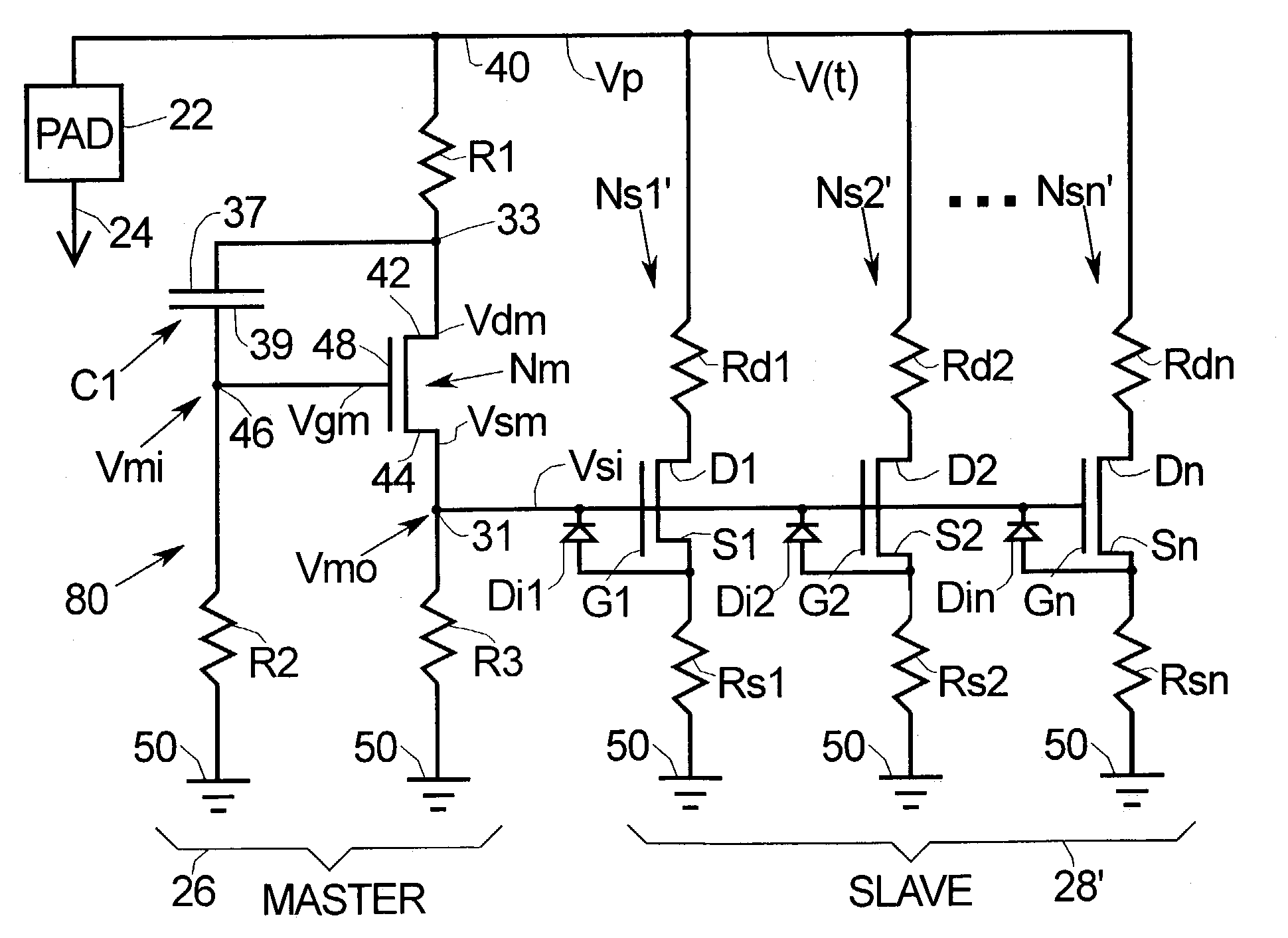
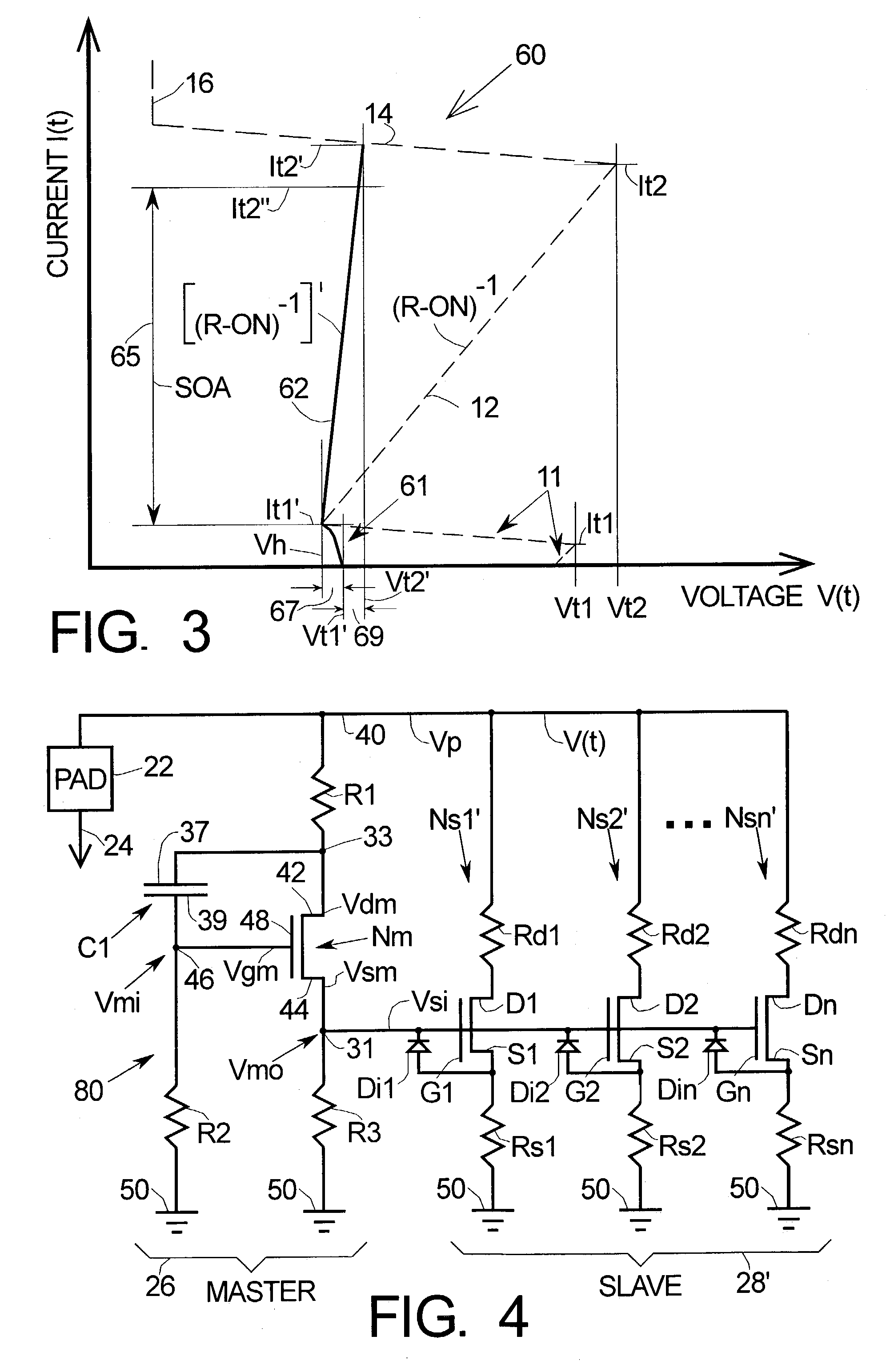
[0035]FIG. 4 is a simplified
schematic diagram illustrating ESD protection arrangement 80 according to a further embodiment of the present invention. Substrate diodes Sb1, Sb2 . . . Sbn are not shown in FIGS. 4–5 for simplicity and convenience of explanation, but persons of skill in the art will understand that they are present. Circuit 80 of FIG. 4 differs from circuit 20 of FIG. 2 in that series drain resistances Rd1, Rd2, . . . Rdn and series source resistances Rs1, Rs2, . . . Rsn are included in slave circuit 28′. Convenient values for these resistances are of the order of 100 to 102 Ohms with about 5 ohms being preferred, but larger or smaller values can also be used. These resistances are useful in equalizing current flow through multiple transistors Ns1, Ns2, . . . Nsn during the ESD event when in conduction regions 61, 62 of FIG. 3. Diodes Di1, Di2, . . . Din are desirably coupled between sources S1, S2, . . . Sn and gates G1, G2, . . . Gn of transistors Ns1, Ns2, . . . N2n, respectively. In the event that master circuit 26 fails to operate for some unexpected reason, for example when transistor Nm has a hidden manufacturing defect, then diodes Di1, Di2, . . . Din will cause transistors Ns1, Ns2, . . . Nsn to turn on in the same way as described in the prior art. Thus diodes Di1, Di2, . . . Din act to increase the overall robustness of the protection circuit of the present invention by providing a fail-safe mode of operation.
[0036]FIG. 5 is a simplified
schematic diagram illustrating ESD suppression circuit 90 according to a still further embodiment of the present invention. The circuit of FIG. 5 has slave portion 28′ like slave portion 28′ of FIG. 4, but slave portion 28 of FIG. 2 could equally well be used. Master portion 26′ of FIG. 5 shows a further embodiment in which master portion 26 of FIG. 2 is replaced by master portion 26′. In master portion 26′, Vmo is generated from V(t)=Vp by means of
Zener diode Z1 and
resistor R4 series coupled between rail 40 and ground 50. Node 31′ at the junction of between Zener Z1 and
resistor R4 and is coupled to gates G1, G2, . . . Gn of slave transistors Ns1′, Ns2′ . . . Nsn′. Slave portion 28, 28′ in FIG. 5 functions in the same manner as slave portions 28, 28′ in FIGS. 2, 4 respectively.
[0037]As the ESD generated voltage V(t) rises, node 31′ remains substantially at ground until Zener Z1 fires at V(t)=Vp. The voltage Vmo appearing on node 31′ is determined by the combination of the Zener voltage of Z1,
resistor R4 and voltage Vp. The use of a zener rather than a
MOSFET in master circuit 26′ can shorten the time required to produce voltage Vmo. It is desirable to choose Z1 and R4 so that when V(t) reaches the level Vp at which it should be clamped, Vmo is sufficient to reduce Vt1 of transistors Ns1, Ns2, . . . Nsn to Vt1′ in much the same way as described in connection with circuits 20, 80 of FIGS. 2, 4. For example, assume that it is desired that ESD protection transistors 28, 28′ fire when V(t)=Vp=about 7 volts, then Z1 and R4 are chosen so that Vmo′ about equals Vt1′ the voltage necessary to reduce Vt1′ to about its minimum value for the transistors of slave circuit 28, 28′. For the example where Vp=˜7 volts, this is about Vmo′=2 to 3 volts and, correspondingly, Z1 is chosen to have a Zener voltage of about 4 to 5 volts. R4 is chosen to limit the current through master circuit 26′ to a sustainable level during the ESD pulse. The Zener voltage needs to be above the normal working voltage of the IC that appears on pad 22 and rail 40 so that master circuit 26′ remains substantially inactive during normal IC operation.
[0038]While at least one exemplary embodiment has been presented in the foregoing

