Solid-state image pickup device and signal processing method therefor

a solid-state image and pickup device technology, applied in the field of solid-state image pickup devices, can solve the problems of difficult to achieve the conversion accuracy of lower voltage, the method is too slow in operation to be made higher, and the optimum a/d conversion is extremely difficult to perform, so as to reduce the size and the price of the image pickup device, and simplify the device construction.

Active Publication Date: 2007-06-05
SONY CORP
View PDF21 Cites 18 Cited by
  • Summary
  • Abstract
  • Description
  • Claims
  • Application Information

AI Technical Summary

Benefits of technology

[0022]The invention has been made in view of the above-described problems, and an object of the invention is to provide a solid-state image pickup device and a signal processing method therefor both of which are capable of performing effective A / D conversion on pixel signals read from pixels and make it possible to achieve a reduction in power consumption and reductions in the size and the price of an image pickup device as well as simplification of the construction of the device, and to realize a high-quality image output.

Problems solved by technology

Although various types of A / D converters to be used for the above-described A / D conversion have heretofore been provided, optimum A / D conversion is extremely difficult to perform, because of the above-described construction in which signal processing circuits each provided for each one of pixel columns or pixel lines perform A / D conversion on pixel signals.
However, this method is too slow in operation to be made higher in conversion accuracy, because the counting operation of the counter takes time, and the error of a comparator easily influences the error of a conversion result and a lower voltage construction is difficult to realize.
For these reasons, the pulse integration type is not suited to A / D conversion to be incorporated into the above-described signal processing part.

Method used


Image

  • Solid-state image pickup device and signal processing method therefor
  • Solid-state image pickup device and signal processing method therefor
  • Solid-state image pickup device and signal processing method therefor

Examples


first embodiment

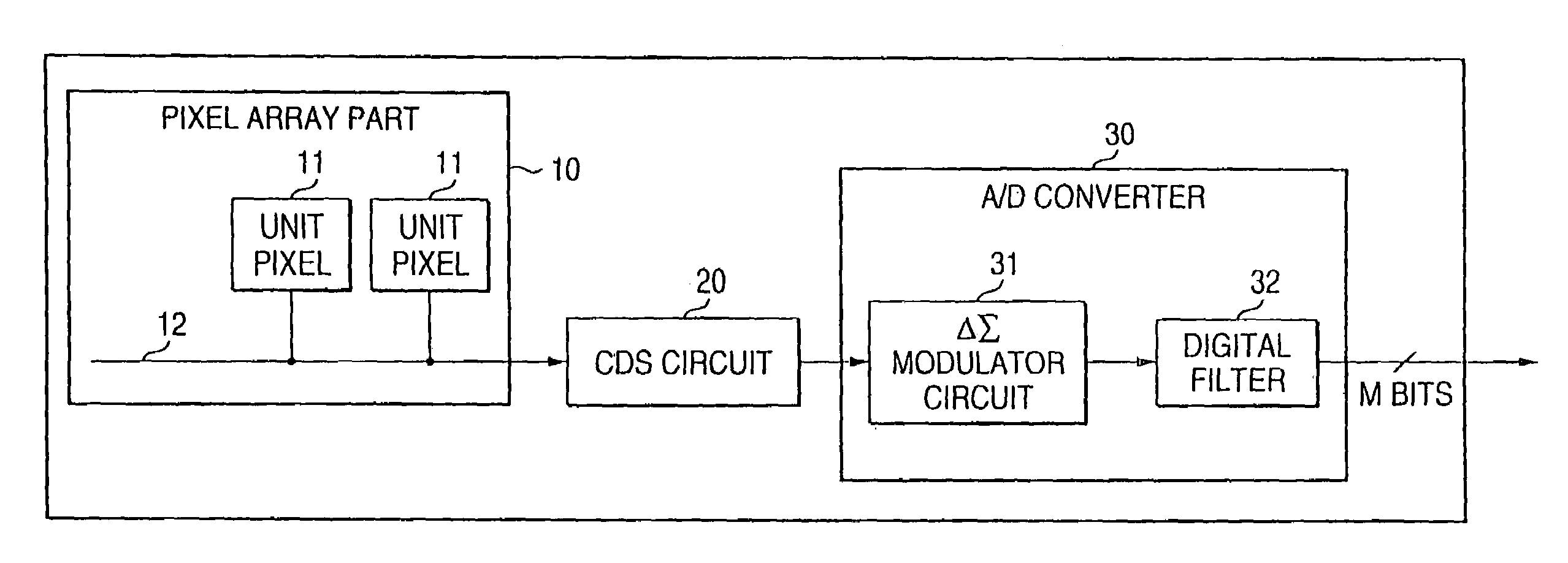
[0064]The basic characteristic portion of the invention resides in the fact that the A / D converter 30 includes a ΔΣ modulator 31 and a digital filter 32.

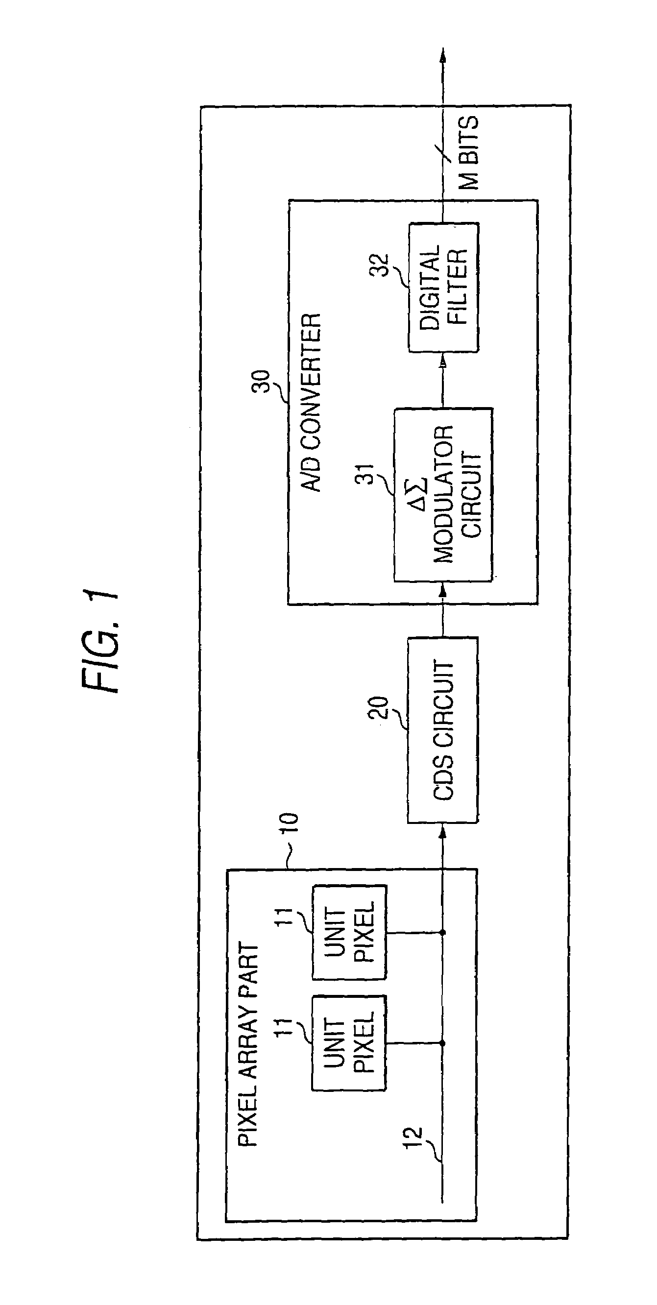
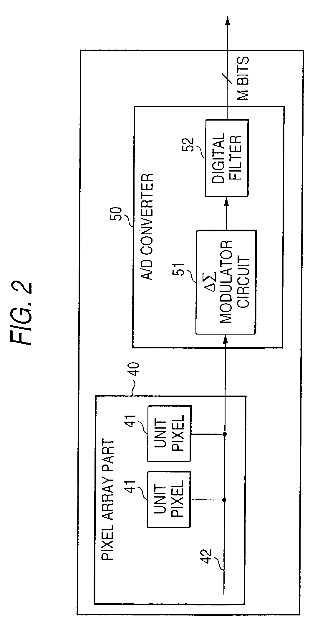
[0065]FIG. 2 shows a pixel array part 40 including a plurality of unit pixels 41 and an A / D converter 50. A pixel signal read from the pixel array part 40 via a signal line 42 is inputted into the A / D converter 50 to perform A / D conversion on the pixel signal. A CDS circuit (not shown in FIG. 2) is provided at the rear stage of the A / D converter 50 so that CDS processing is performed on the pixel signal converted into a digital signal.

second embodiment

[0066]The basic characteristic portion of the invention resides in the fact that the A / D converter 50 includes a ΔΣ modulator 51 and a digital filter 52.

[0067]The main difference between the constructions shown in FIGS. 1 and 2 is that the order of arrangement of the CDS circuit 20 and the A / D converter 30. is opposite to the order of arrangement of the CDS (not shown) and the A / D converter 50, and the A / D converters 30 and 50 which constitute part of the respective basic characteristic portions have a common construction.

[0068]FIG. 1 shows the construction of one of the pixel columns, and the pixel array part 10 is constructed to output pixel signals in the respective pixel columns via the corresponding signal lines, and the CDS circuit 20 and the A / D converter 30 are provided for each of the pixel columns and are constructed as part of a so-called column type of signal processing unit which performs signal processing on pixel signals in units of pixel columns.

[0069]In general, an ...

third embodiment

[0143]the invention will be described below.

[0144]FIG. 12 is a block diagram showing an essential portion of a solid-state image pickup device according to the third embodiment of the invention. In FIG. 12, the same reference numerals are used to denote the same constituent elements as those used in the solid-state image pickup device shown in FIG. 1.

[0145]The solid-state image pickup device according to the third embodiment has a construction in which output control circuits 60 for sequentially selecting digital pixel signals converted by the above-described plurality of A / D converters and outputting the sequentially selected digital pixel signals in their line directions are provided at the rear stage of the above-described A / D converter.

[0146]The respective output control circuits 60 are circuits for sequentially transferring digital pixel signals outputted from the corresponding digital filters 32 of the A / D converters 30 in the pixel-line directions, and are capable of outputti...


PUM


Abstract

The invention makes it possible to perform effective A / D conversion on pixel signals read from a pixel array part, to achieve a reduction in power consumption and reductions in the size and the price of an image pickup device as well as simplification of the construction of the device, and to realize a high-quality image output. The device includes an pixel array part having a plurality of unit pixels, a CDS (correlated double sampling) circuit, and an A / D converter. A pixel signal read from a pixel array part via a signal line is subjected to CDS processing (noise elimination processing) in the CDS circuit, and then this pixel signal is inputted into the A / D converter which performs A / D conversion on the pixel signal. The A / D converter includes a ΔΣ modulator and a digital filter to perform highly accurate A / D conversion. The invention can also be applied to a construction in which an A / D converter is provided at the front stage of the CDS circuit.

Description

BACKGROUND OF THE INVENTION[0001]1. Field of the Invention[0002]The present invention relates to a solid-state image pickup device which performs A / D conversion on pixel signals generated in a pixel array part formed of a plurality of photoelectric conversion elements and outputs the obtained digital pixel signals, and more particularly, to a solid-state image pickup device including improved A / D converters for pixel signals, a signal processing method for such a solid-state image pickup device, and an electronic apparatus or electronic equipment including such a solid-state image pickup device. The term “electronic apparatus or electronic equipment” indicates, for example, a digital camera, a mobile telephone with a camera, or a personal computer, and the term “solid-state image pickup device” indicates an image pickup chip for a CCD image pickup device or an amplification type image pickup device (CMOS sensor), or an electronic device module in which an image pickup chip is integr...

Claims


Application Information

Patent Timeline
Patent Type & Authority Patents(United States)
IPC IPC(8): H04N5/228H01L27/146H04N5/14H04N5/335H04N5/357H04N5/363H04N5/369H04N5/372H04N5/374H04N5/378
CPCH04N5/335H04N25/00H04N25/57H04N25/60H04N25/75
Inventor SATO, HIROKIMABUCHI, KEIJINAKAMURA, NOBUOIIZUKA, TETSUYA
Owner SONY CORP
Why Eureka
Try Eureka