Magnetic detecting element having pinned magnetic layers disposed on both sides of free magnetic layer

a magnetic layer and detecting element technology, applied in the field of magnetic detecting elements, can solve problems such as difficulty in further shortening the gap length, and achieve the effect of increasing the difference between the ease of conduction electron flow and increasing the resistance change r

Inactive Publication Date: 2007-06-12
TDK CORPARATION
View PDF8 Cites 21 Cited by
  • Summary
  • Abstract
  • Description
  • Claims
  • Application Information

AI Technical Summary

Benefits of technology

[0028]The present invention has been achieved for solving the above problems of the conventional magnetic detecting elements, and an object of the present invention is to provide a magnetic detecting element capable of increasing a difference between the ease of a conduction electron flow in a low-resistance state and the ease of a conduction electron flow in a high-resistance state, for increasing a change ΔR in resistance.

Problems solved by technology

However, in the system in which the free magnetic layer, the nonmagnetic material layer and the pinned magnetic layer are laminated in the direction perpendicular to the film plane, it is difficult to further shorten the gap length.
However, the magnetic detecting element shown in FIG. 14 causes the following problem.
However, the magnetic detecting element shown in FIG. 26 causes the following problem.

Method used


Image

  • Magnetic detecting element having pinned magnetic layers disposed on both sides of free magnetic layer
  • Magnetic detecting element having pinned magnetic layers disposed on both sides of free magnetic layer
  • Magnetic detecting element having pinned magnetic layers disposed on both sides of free magnetic layer

Examples


second embodiment

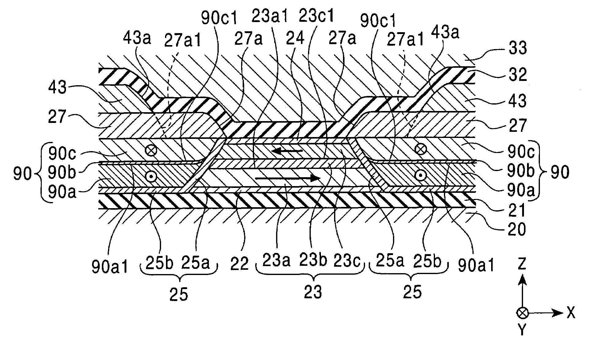
[0181]FIG. 2 is a partial sectional view showing the structure of a magnetic detecting element according to the present invention, as viewed from a surface facing a recording medium. In FIG. 2, a layer denoted by the same reference numeral as in FIG. 1 comprises the same material and has the same thickness and shape as those of the corresponding layer shown in FIG. 1 unless otherwise specified.

[0182]The magnetic detecting element shown in FIG. 2 is different from that shown in FIG. 1 in that hard bias layers are not formed on the outsides of the respective pinned magnetic layers 26, but a ferromagnetic layer 41 and an antiferromagnetic layer 42 are laminated on the free magnetic layer 23 through a separating layer 40 comprising alumina.

[0183]An exchange anisotropic magnetic field is produced at the interface between the ferromagnetic layer 41 and the antiferromagnetic layer 42 to pin magnetization of the ferromagnetic layer 41 in the X direction shown in the drawing. Furthermore, ma...

third embodiment

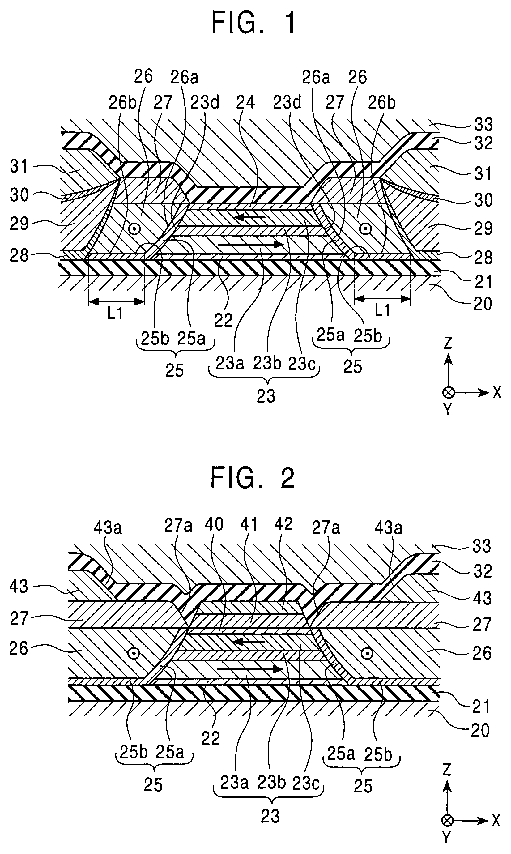
[0185]FIG. 3 is a partial sectional view showing the structure of a magnetic detecting element according to the present invention, as viewed from a surface facing a recording medium. In FIG. 3, a layer denoted by the same reference numeral as in FIG. 1 comprises the same material and has the same thickness and shape as those of the corresponding layer shown in FIG. 1 unless otherwise specified.

[0186]The magnetic detecting element shown in FIG. 3 is different from that shown in FIG. 1 in that hard bias layers are not formed on the outsides of the respective pinned magnetic layers 26, but an underlying layer 51 and a hard magnetic layer 52 are laminated on the free magnetic layer 23 through a separating layer 50 comprising alumina.

[0187]The underlying layer 51 comprises Cr, Ta or a Ta / Cr laminated film, and the hard magnetic layer 52 comprises Co—Pt. The hard magnetic layer 52 is magnetized in the X direction. Furthermore, magnetostatic coupling occurs between the hard magnetic layer ...

fourth embodiment

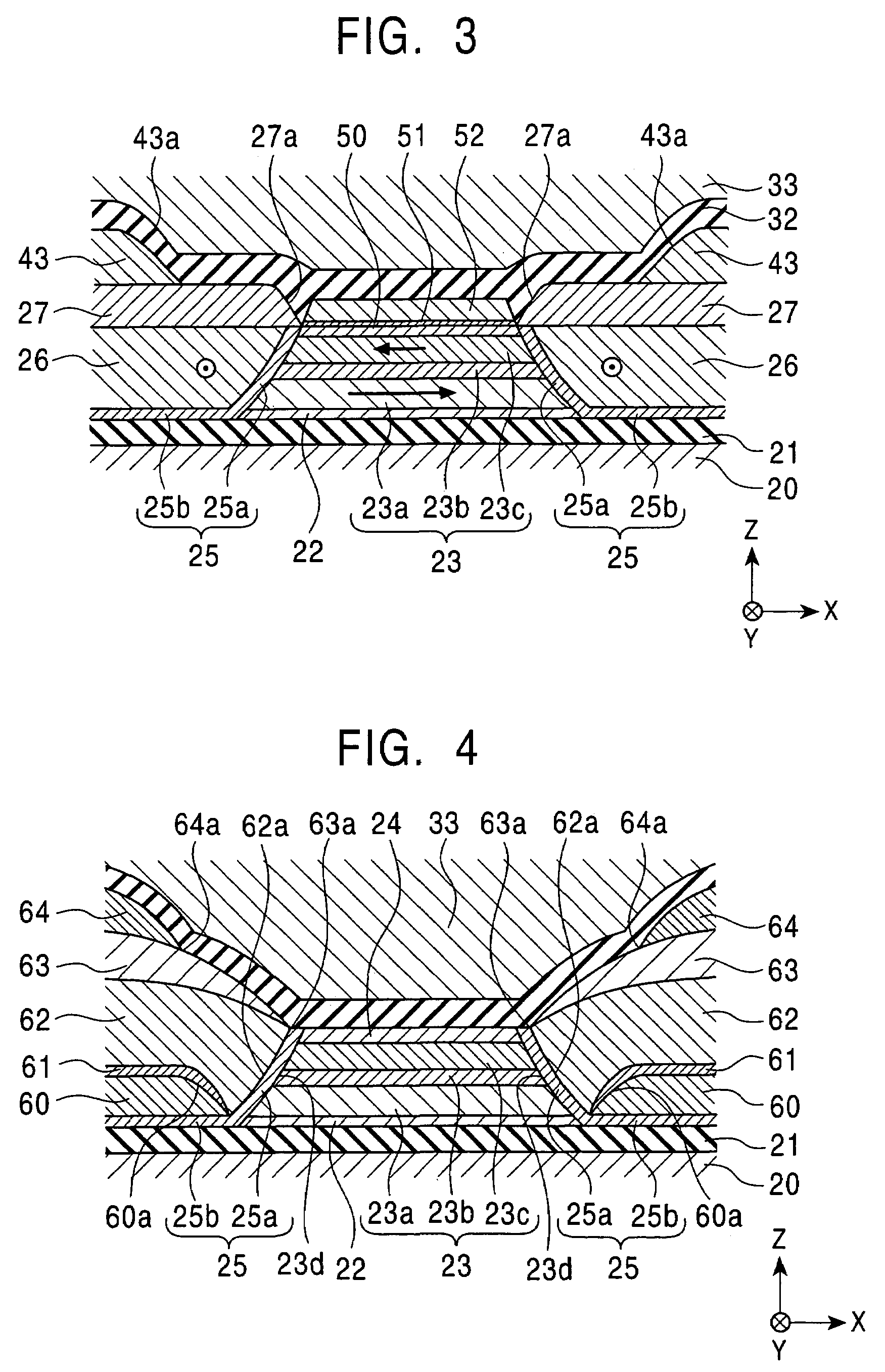
[0191]FIG. 4 is a partial sectional view showing the structure of a magnetic detecting element according to the present invention, as viewed from a surface facing a recording medium. In FIG. 4, a layer denoted by the same reference numeral as in FIG. 1 comprises the same material and has the same thickness and shape as those of the corresponding layer shown in FIG. 1 unless otherwise specified.

[0192]The magnetic detecting element shown in FIG. 4 is different from that shown in FIG. 1 in that separating layers 61 comprising a nonmagnetic material, pinned magnetic layers 62, antiferromagnetic layers 63 and electrode layers 64 are laminated in that order on respective hard bias layers 60 formed on both sides of the free magnetic layer 23.

[0193]Each of the hard bias layers 60 has an inclined or curved inner end surface 60a. Therefore, the thickness of each hard bias layer 60 gradually decreases nearer to the free magnetic layer 23. With the hard bias layers 60 each having such a tapered...


PUM

PropertyMeasurementUnit
track widthaaaaaaaaaa
blocking temperatureaaaaaaaaaa
temperatureaaaaaaaaaa

Abstract

The present invention provides a magnetic detecting element capable of increasing a difference between the ease of a conduction electron flow in a low-resistance state and the ease of a conduction electron flow in a high-resistance state to increase a resistance change ΔR. In the magnetic detecting element, a free magnetic layer or a pinned magnetic layer has a synthetic ferromagnetic structure including a first free magnetic sub-layer or a first pinned magnetic sub-layer containing a magnetic material having a positive β value, and a second magnetic sub-layer or a second pinned magnetic sub-layer containing a magnetic material having a negative β value. The β value is characteristics of a magnetic material satisfying the relationship ρ↓/ρ↑=(1+β)/(1−β)(−1≦β≦1)(wherein ρ↓ represents resistivity for minority conduction electrons, and ρ↑ represents resistivity for majority conduction electrons).

Description

[0001]This application claims the benefit of priority to Japanese Patent Application Nos. 2003-006626 and 2003-006627, herein incorporated by reference.BACKGROUND OF THE INVENTION[0002]1. Field of the Invention[0003]The present invention relates to a magnetic detecting element comprising pinned magnetic layers adjacent to both end surfaces of a free magnetic layer through nonmagnetic material layers so that a sense current flows in a direction crossing the interfaces between the free magnetic layer and the nonmagnetic material layers and the interfaces between the pinned magnetic layers and the nonmagnetic material layers. Particularly, the present invention relates to a magnetic detecting element capable of effectively improving a rate ΔR / R of change in resistance.[0004]2. Description of the Related Art[0005]With improvements in the linear recording density of a recording medium there have recently been demands for a shorter gap length. The gap length is defined by a distance betwe...

Claims


Application Information

Patent Timeline
Patent Type & Authority Patents(United States)
IPC IPC(8): G11B5/39G11B5/127G01R33/09G11B5/00G11B5/31H01F10/32
CPCB82Y10/00B82Y25/00G01R33/093G11B5/3903H01F41/325H01F10/3277G11B5/3932G11B5/313G11B2005/0016Y10T428/1143Y10T428/115Y10T428/1121
Inventor HASEGAWA, NAOYASAITO, MASAMICHI
Owner TDK CORPARATION
Why Eureka
Try Eureka