Automated sourcing of substrate microfabrication defects using defects signatures

a microfabrication and defect technology, applied in the detection of semiconductor fabrication defects, semiconductor/solid-state device testing/measurement, instruments, etc., can solve the problems of human identification of defect source, primitive detection of defect signature, and laborious and time-consuming effor

Inactive Publication Date: 2007-06-12
SIGLAZ +1
View PDF9 Cites 30 Cited by
  • Summary
  • Abstract
  • Description
  • Claims
  • Application Information

AI Technical Summary

Problems solved by technology

Drawbacks of this approach include: (a) defect signature recognition is primitive, and flags are raised too late and after yields have already dropped; (b) identification of the defect source is done by humans and represents a tedious and time consuming effort; and (c) successful defect sourcing depends on expert know-how that is difficult to capture.

Method used


Image

  • Automated sourcing of substrate microfabrication defects using defects signatures
  • Automated sourcing of substrate microfabrication defects using defects signatures
  • Automated sourcing of substrate microfabrication defects using defects signatures

Examples


Embodiment Construction

[0052]The following definitions serve as a glossary of terms as used herein:

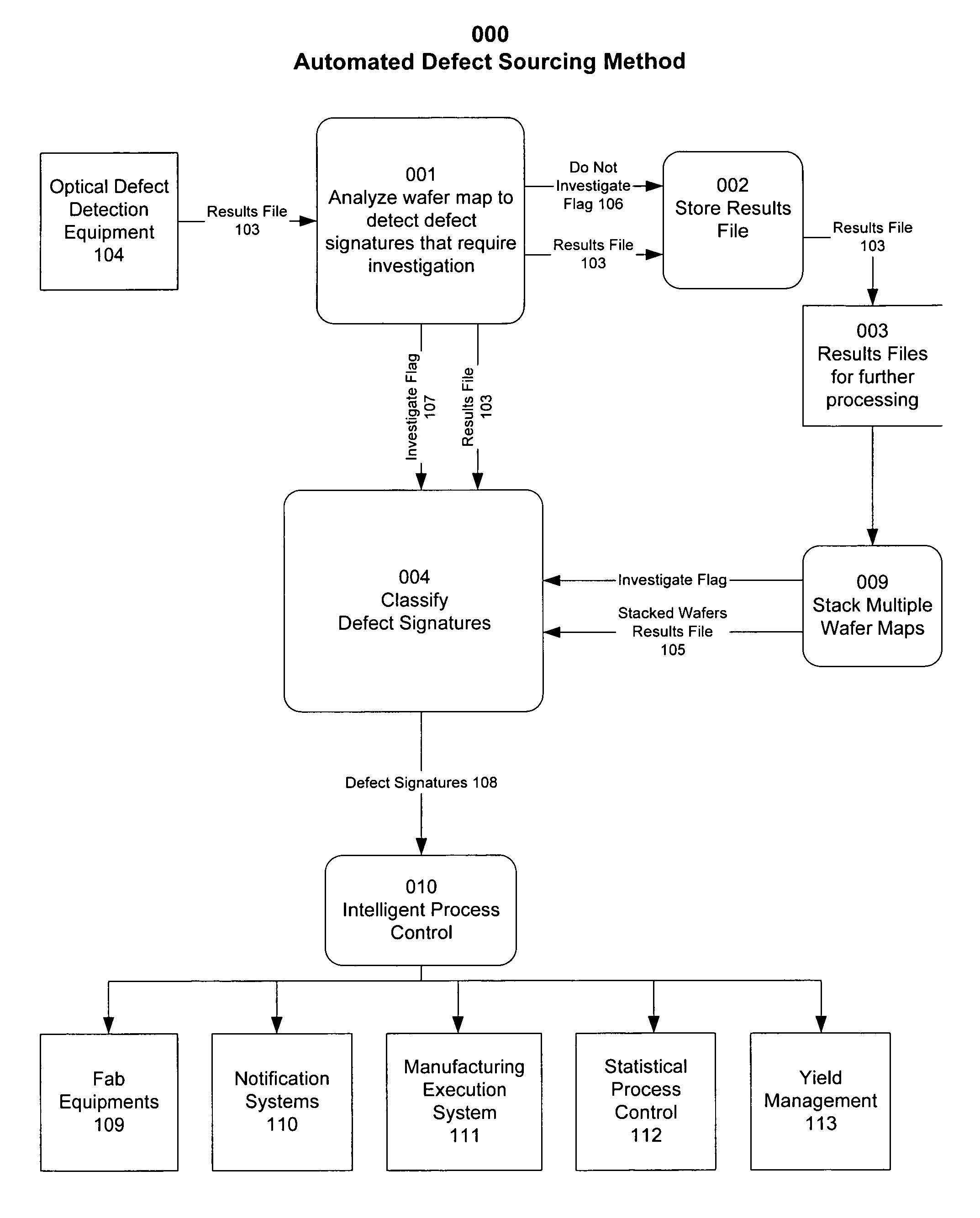
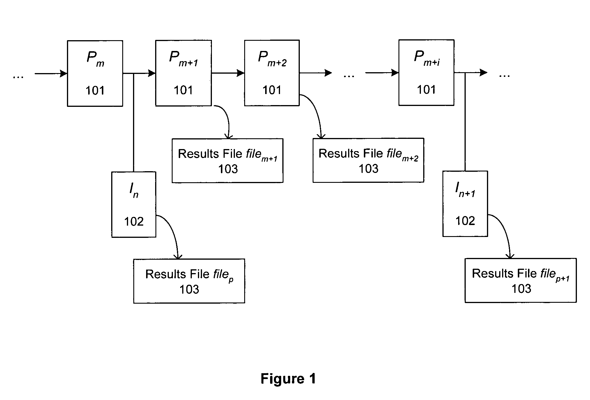
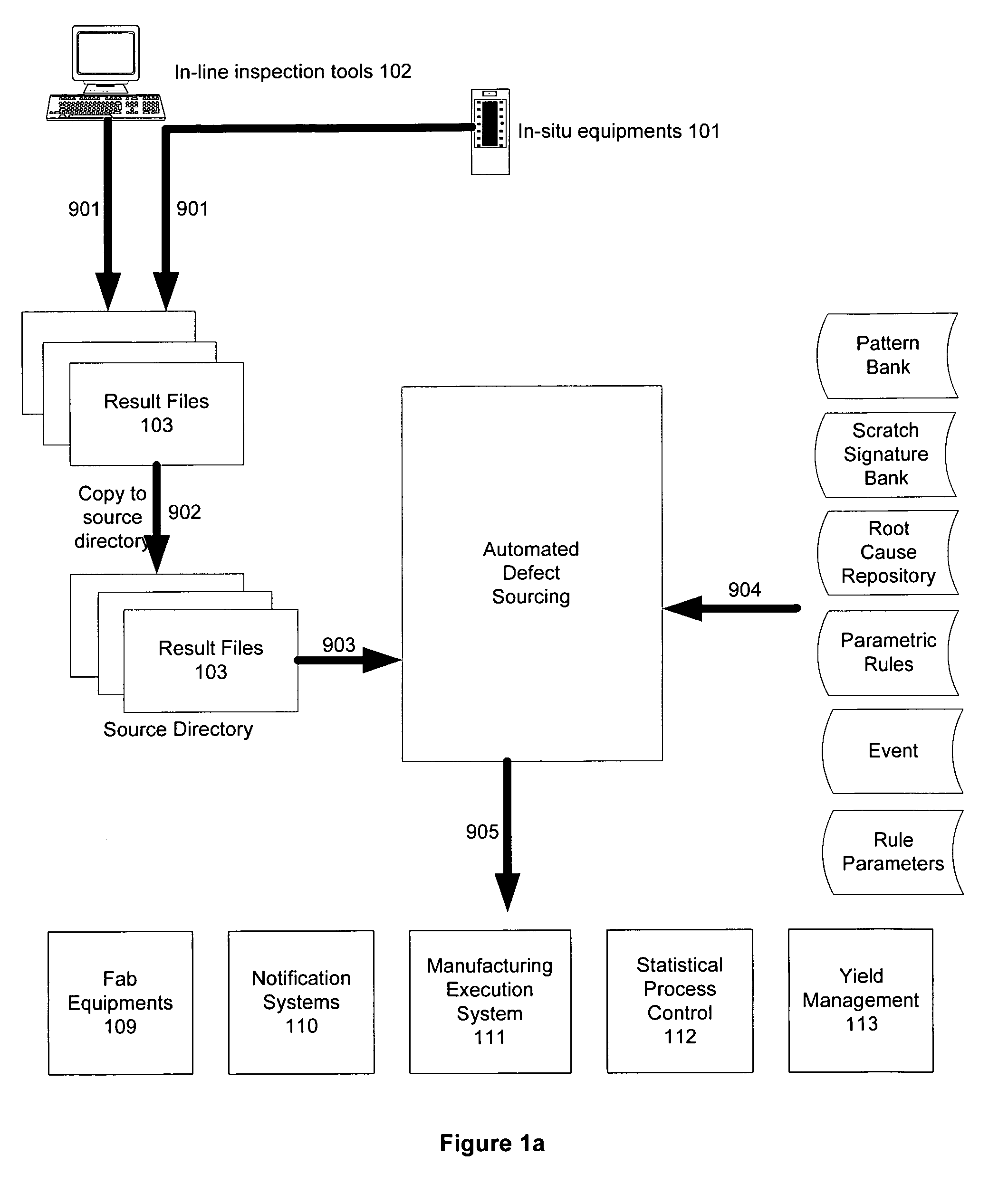
[0053]Defect: A pit, tear, groove, inclusion, grain boundary, or other surface feature anomaly that is either characteristic of the material or a result of its processing and that is not a result of the sample preparation. (examples: particle deposited on substrate; scratch / streak on wafer; lithographic error; non-uniform deposition, etch or planarization; excessive or inadequate deposition, etch or planarization).

Defect Cluster: A grouping of defects detected on a wafer surface that have commonality in position, size, orientation and / or one or more other measurable attributes.

Concentrated cluster: A dense grouping of non-random defects that comprises micro-clusters, scratch clusters and repeating litho clusters.

Micro-cluster: A grouping of concentrated defects contained totally with a single die. When an envelope is drawn around the micro-cluster, the major axis of the envelope is much smaller than both the...


PUM


Abstract

Automated defect sourcing system identifies root-causes of yield excursion due to contamination, process faults, equipment failure and/or handling in timely manner and provides accurate timely feedback to address and contain the sources of yield excursion. A signature bank stores known wafer surface manufacturing defects as defect signatures. The signature of a manufacturing defect pattern is associated with a type of equipment or process, and used to source the manufacturing defects and to provide process control for changing and/or stopping yield excursion during fabrication. A defect signature recognition engine matches wafer defects against the signature bank during wafer fabrication. Once the defect signature is detected during fabrication, handling and/or disposing the root-cause of the corresponding defect is facilitated using messages according to an event handling database. Optionally, a real-time process control for wafer fabrication is provided.

Description

BACKGROUND[0001]1. Field[0002]Invention relates to detection of semiconductor fabrication defects, and in particular to a method and system for predictive, automatic and self-learning semiconductor fabrication defect signature recognition and defect sourcing.[0003]2. Related Art[0004]Conventional semiconductor fabrication systems incorporate statistical process control and impose control limits on the acceptable number of defects on a wafer, detect quantity of defects on a given wafer, and raise a flag if the quantity falls out of bounds. Defective wafers are inspected by human experts in the hope of pinpointing the fabrication process steps responsible for the defect. Drawbacks of this approach include: (a) defect signature recognition is primitive, and flags are raised too late and after yields have already dropped; (b) identification of the defect source is done by humans and represents a tedious and time consuming effort; and (c) successful defect sourcing depends on expert know...

Claims


Application Information

Patent Timeline
Patent Type & Authority Patents(United States)
IPC IPC(8): H01L21/66
CPCG06Q50/04Y02P90/30
Inventor LUU, VICTOR V.POREDA, JOHN
Owner SIGLAZ
Why Eureka
Try Eureka