Integrated circuit chip utilizing dielectric layer having oriented cylindrical voids formed from carbon nanotubes

a carbon nanotube and integrated circuit technology, applied in the direction of electrical equipment, semiconductor devices, semiconductor/solid-state device details, etc., can solve the problems of difficult to ensure, the designer's parasitic capacitance becomes a significant problem, and the clock speed is necessarily limited, so as to reduce the dielectric constant

Inactive Publication Date: 2007-06-12
GLOBALFOUNDRIES INC
View PDF7 Cites 24 Cited by
  • Summary
  • Abstract
  • Description
  • Claims
  • Application Information

AI Technical Summary

Benefits of technology

[0014]A dielectric structure (preferably as a layer of an integrated circuit chip) is formed by creating oriented cylindrical voids in a conventional dielectric material, such as silicon oxide. The voids reduce the dielectric constant of the composite structure below that of a conventional solid dielectric.
[0018]The use of a conventional dielectric material having numerous air voids, as described herein, provides a relatively low-k dielectric. Furthermore, because the material is conventional (e.g., silicon oxide), any of various conventional processes can be used for depositing, polishing, patterning, etching, or otherwise manufacturing the integrated circuit wafer. Carbon nanotubes can be grown very thin and elongated, in a dense pattern. Unlike certain previous attempts to introduce air voids into a dielectric material, the use of carbon nanotubes produces oriented cylindrical voids of sufficient number to substantially reduce the dielectric constant of the resultant structure, leaving a dielectric layer which is both structurally strong and can be constructed compatibly with conventional processes and with other structures in the integrated circuit.

Problems solved by technology

Clock speeds are necessarily limited by various design parameters, and in particular are limited by signal propagation delays.
Early computer processors, which were constructed from many discrete components, were susceptible to significant speed improvements by shrinking component size, reducing discrete component numbers, and eventually, packaging the entire processor as an integrated circuit on a single chip.
As the number of such conductors increases and as processor clock speeds also increase, this parasitic capacitance becomes a significant problem for the designer.
I.e., it becomes increasingly difficult to assure that all required signals will propagate the full length of their conductors and cause any required state change in an element at the opposite end within the available clock cycle time.
However, it is not possible to simply select any arbitrary low-k material as a dielectric.
However, all such materials have their respective drawbacks, such as compatibility with existing processes or semiconductor materials.
No single dielectric material has emerged as a clearly superior alternative to conventional silicon oxide.

Method used


Image

  • Integrated circuit chip utilizing dielectric layer having oriented cylindrical voids formed from carbon nanotubes
  • Integrated circuit chip utilizing dielectric layer having oriented cylindrical voids formed from carbon nanotubes
  • Integrated circuit chip utilizing dielectric layer having oriented cylindrical voids formed from carbon nanotubes

Examples


Embodiment Construction

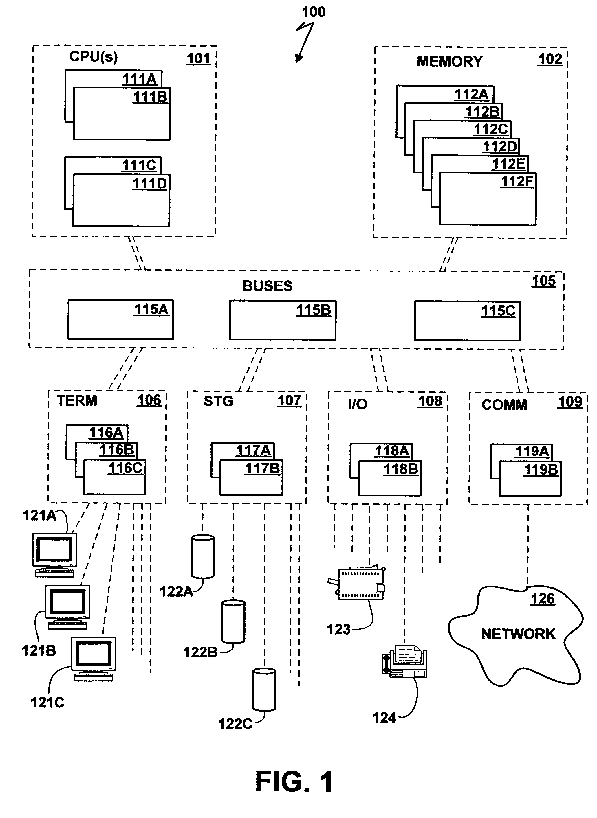
[0026]Referring to the Drawing, wherein like numbers denote like parts throughout the several views, FIG. 1 is a high-level representation of the major hardware components of a computer system 100 for utilizing integrated circuits having carbon nanotube conductors, according to the preferred embodiment of the present invention. At a functional level, the major components of system 100 are shown in FIG. 1 outlined in dashed lines; these components include one or more central processing units (CPU) 101, main memory 102, terminal interface 106, storage interface 107, I / O device interface 108, and communications / network interfaces 109, all of which are coupled for inter-component communication via one or more buses 105.

[0027]CPU 101 is one or more general-purpose programmable processors, executing instructions stored in memory 102; system 100 may contain either a single CPU or multiple CPUs, either alternative being collectively represented by feature CPU 101 in FIG. 1, and may include ...


PUM

PropertyMeasurementUnit
dielectric constantaaaaaaaaaa
depthaaaaaaaaaa
thickaaaaaaaaaa

Abstract

A dielectric in an integrated circuit is formed by creating oriented cylindrical voids in a conventional dielectric material. Preferably, voids are formed by first forming multiple relatively long, thin carbon nanotubes perpendicular to a surface of an integrated circuit wafer, by depositing a conventional dielectric on the surface to fill the area between the carbon nanotubes, and by then removing the carbon nanotubes to produce voids in place of the carbon nanotubes. A layer of dielectric and voids thus formed can be patterned or otherwise processed using any of various conventional processes. The use of a conventional dielectric material having numerous air voids substantially reduces the dielectric constant, leaving a dielectric structure which is both structurally strong and can be constructed compatibly with conventional processes and materials.

Description

FIELD OF THE INVENTION[0001]The present invention relates to digital data processing, and in particular to the design of integrated circuit chips used as components of digital data systems.BACKGROUND OF THE INVENTION[0002]In the latter half of the twentieth century, there began a phenomenon known as the information revolution. While the information revolution is a historical development broader in scope than any one event or machine, no single device has come to represent the information revolution more than the digital electronic computer. The development of computer systems has surely been a revolution. Each year, computer systems become faster, store more data, and provide more applications to their users.[0003]A modern computer system typically comprises a central processing unit (CPU) and supporting hardware necessary to store, retrieve and transfer information, such as communications buses and memory. It also includes hardware necessary to communicate with the outside world, s...

Claims


Application Information

Patent Timeline
Patent Type & Authority Patents(United States)
IPC IPC(8): H01L21/00
CPCB82Y10/00H01L21/7682H01L23/5222H01L23/5329H01L23/53238H01L2924/0002Y10S977/742Y10S977/842H01L2924/00
Inventor FURUKAWA, TOSHIHARUHAKEY, MARK CHARLESHOLMES, STEVEN JOHNHORAK, DAVID VACLAVKOBURGER, III, CHARLES WILLIAMMITCHELL, PETER H.
Owner GLOBALFOUNDRIES INC
Why Eureka
Try Eureka