Apparatus for reducing signal reflection in a circuit board

Inactive Publication Date: 2007-06-12
CISCO TECH INC
View PDF11 Cites 21 Cited by
  • Summary
  • Abstract
  • Description
  • Claims
  • Application Information

AI Technical Summary

Benefits of technology

[0053]The offset distance 90 between the pad center axis 72 and the opening center axis 74 aligns the portion 97 of the opening 70 with the contact pad 42 and aligns the portion 98 of the second conductive layer 36 with the contact pad 42. Alignment of the portion 98 of the second conductive layer 36 with the contact pad 42 (e.g., along the y-axis direction 16) is illustrated as shaded area 99. During operation of the circuit board 30, for example, as current 102 travels through the signal conductor 40 and reaches the contact pad 42, the current 102 travels through the portion of the contact pad 42 within the shaded area 99 (e.g., the portion of the contact pad 42 aligned with, along the y-axis 16, the portion 98 of the second signal layer 36). Orientation of the portion 97 of the opening 70 and the portion 98 of the second signal layer 36 relative to the contact pad 42 effectively reduces the width 58 (e.g., area) of the contact pad 42 relative to the width 60 of the signal conductor 40. Such reduction of the width 58 of the cont

Problems solved by technology

Conventional techniques for utilizing conductive pads of a circuit board suffer from

Method used


Image

  • Apparatus for reducing signal reflection in a circuit board
  • Apparatus for reducing signal reflection in a circuit board
  • Apparatus for reducing signal reflection in a circuit board

Examples


Embodiment Construction

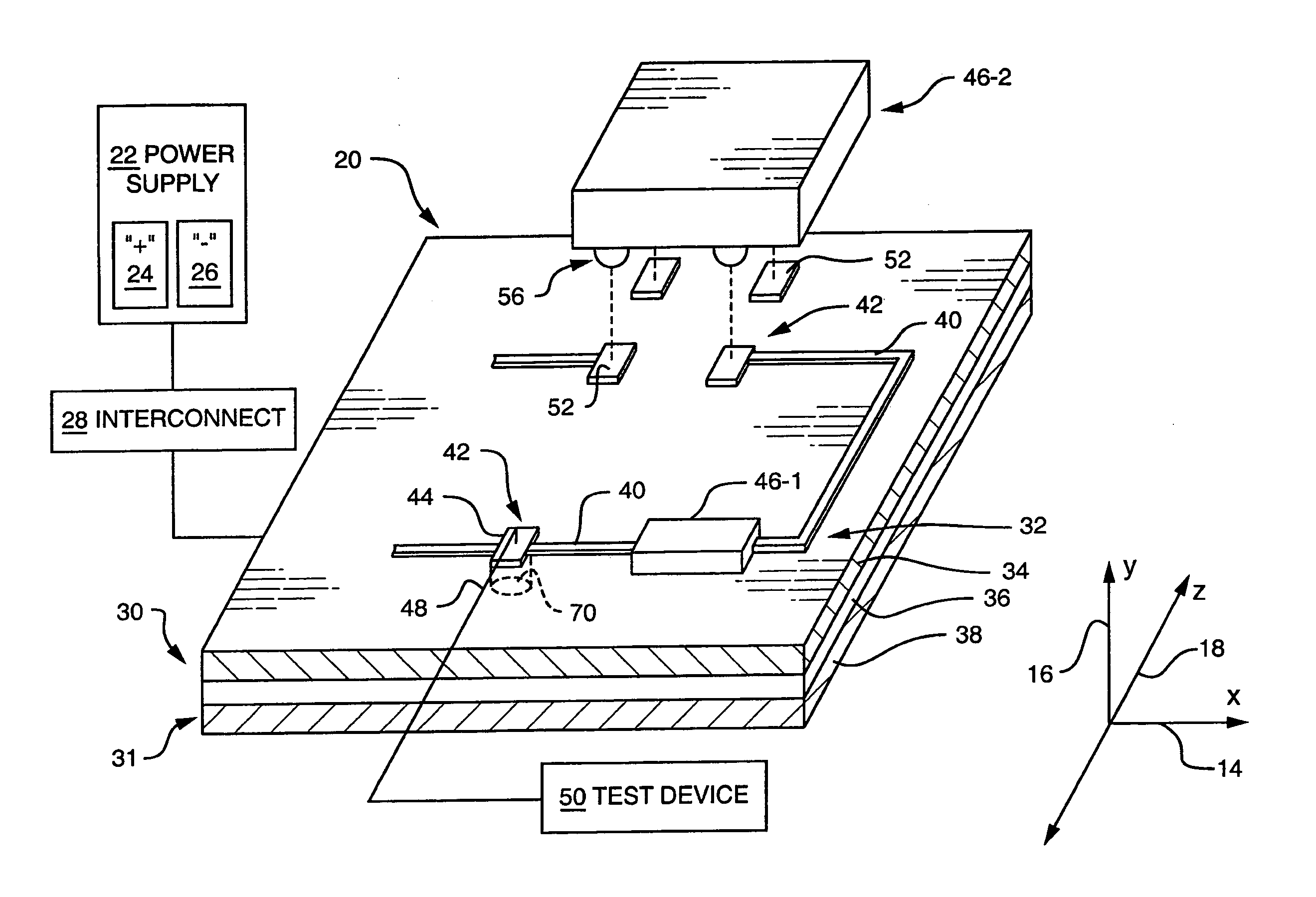
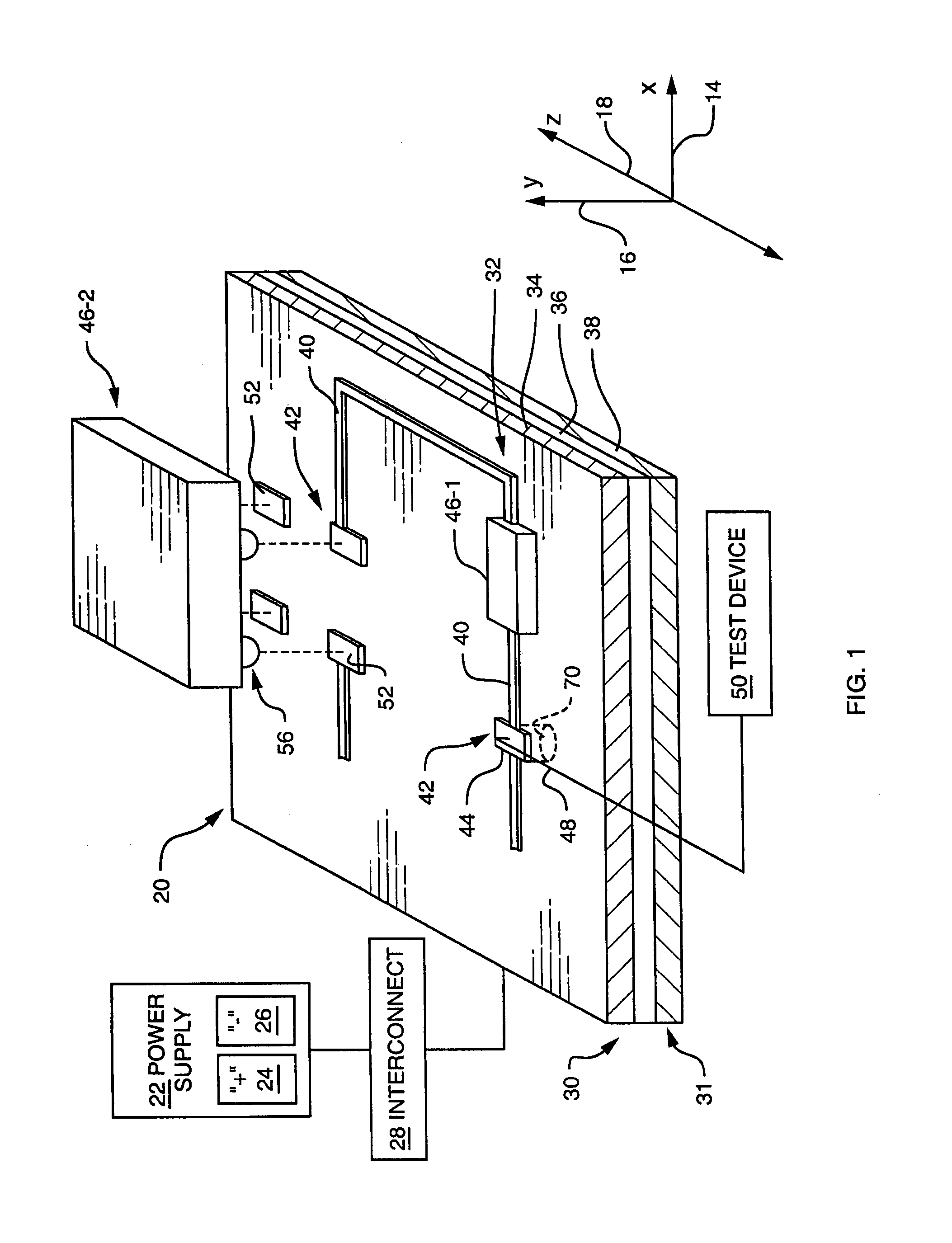
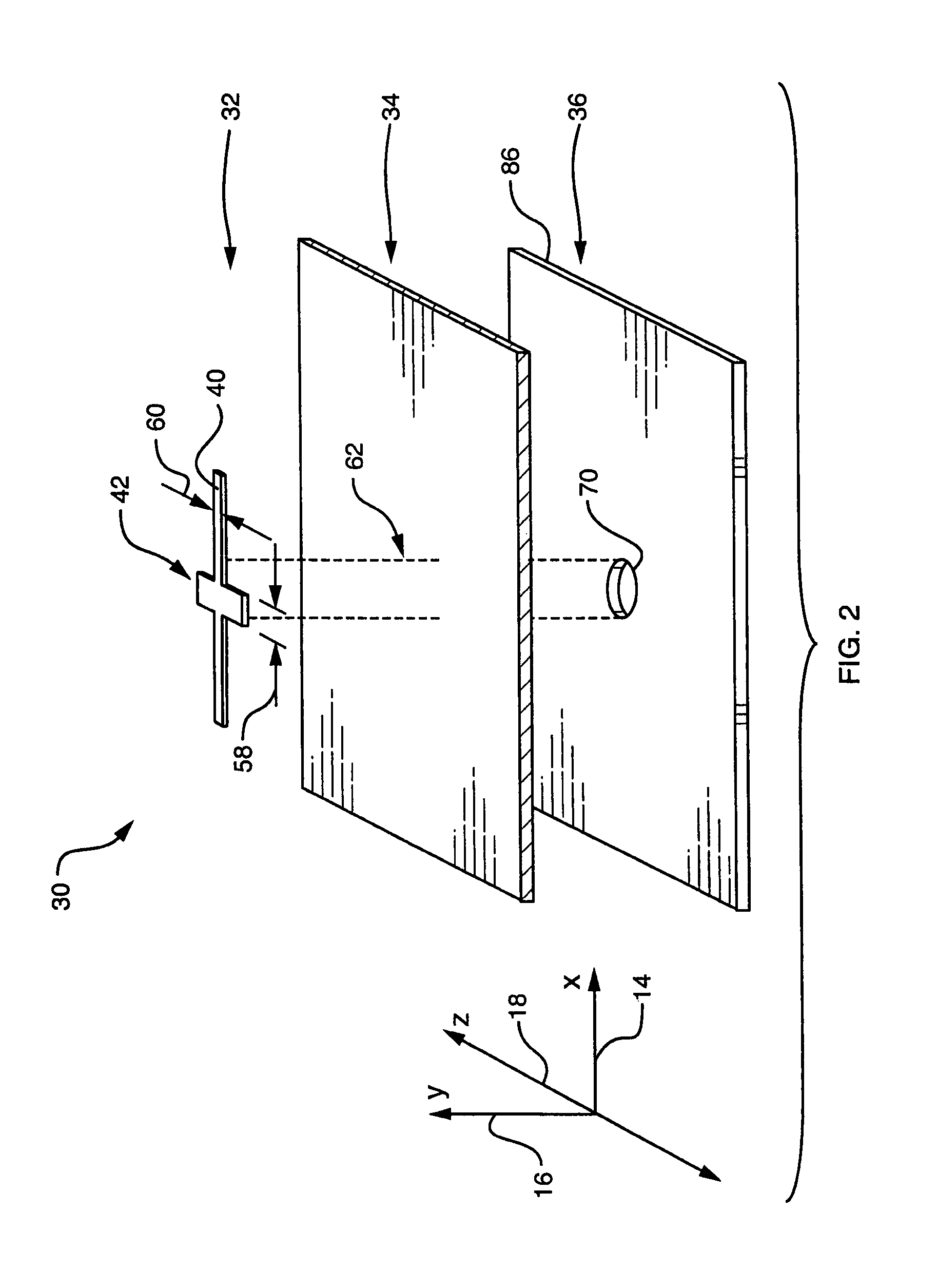
[0029]Embodiments of the present invention provide mechanisms for minimizing an impedance mismatch between a signal conductor (e.g., conductive trace) and a contact pad (e.g., conductive pad) on a circuit board to minimize signal reflection of a signal transmitted through the signal conductor and across the contact pad, thereby reducing signal loss. The circuit board has, in a first signal layer, the signal conductor having a relatively small width and the contact pad having a relatively large width. The relatively large width of the contact pad combined with the relatively narrow signal conductor creates an impedance mismatch between the contact pad and the signal conductor. The circuit board has, in a second signal layer, a ground plane separated from the first signal layer by a nonconductive layer. The circuit board defines an opening in the second signal layer underneath the contact pad. The presence of the ground plane underneath the contact pad typically affects the impedance ...


PUM


Abstract

A circuit board has, in a first signal layer, a signal conductor having a relatively small width and a contact pad having a relatively large width. The relatively large width of the contact pad combined with the relatively narrow signal conductor creates an impedance mismatch between the contact pad and the signal conductor. The circuit board has, in a second signal layer, a ground plane separated from the first signal layer by a nonconductive layer. The circuit board defines an opening in the second signal layer underneath the contact pad. The presence of the ground plane underneath the contact pad typically affects the impedance of the contact pad. The opening in the second signal layer removes a portion the ground plane relative to the contact pad and, therefore, reduces the impedance mismatch between the contact pad and the signal conductor. Such reduction in the mismatch of the impedances between the contact pad and the signal conductor minimizes signal reflection of a signal transmitted through the signal conductor and across the contact pad.

Description

BACKGROUND[0001]A typical circuit board includes layers of conductive material (e.g., copper) and nonconductive material (e.g., fiberglass) sandwiched together to form a single, rigid board. Some circuit boards include many layers of alternating conductive and nonconductive materials.[0002]In general, to manufacture a circuit board having multiple layers, a circuit board manufacturer creates separate circuit board sheets. Each circuit board sheet typically includes two conductive signal layers and a nonconductive separating layer disposed between the conductive signal layers. The manufacturer typically aligns multiple circuit board sheets along with other nonconductive sheets (e.g., nonconductive core layers) in an interleaved manner and laminates the sheets to form a single, integrated board.[0003]A typical circuit board includes, as one of the signal layers, ground planes and power planes to provide power to the circuitry of the circuit board (e.g., circuit board components). A gr...

Claims


Application Information

Patent Timeline
IPC IPC(8): H05K1/11H05K1/14
CPCH05K1/0224H05K1/025H05K1/0268H05K1/111H05K1/0237H05K2201/0792H05K2201/09236H05K2201/09281H05K2201/093H05K2201/0969Y02P70/50
Inventor AHMAD, BILAL
Owner CISCO TECH INC
Why Eureka
Try Eureka